
Control Unit
Overview
- Purpose: The Control Unit is the orchestrating component of DigiSim's 8-bit computer architecture. It generates the control signals necessary to coordinate the Program Counter, Memory (RAM), Instruction Register, ALU, Flags Register, and other components to execute a complete instruction set.
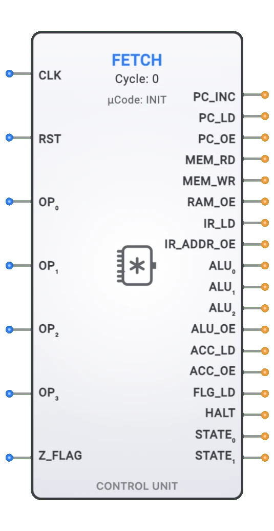
- Symbol: The Control Unit is represented by a rectangular block with multiple input and output pins for interfacing with the various CPU components.
- DigiSim.io Role: The Control Unit enables the creation of a complete, functional 8-bit computer by properly sequencing and controlling all system components through a fetch-decode-execute-store cycle.
Functional Description
State Machine Operation
The Control Unit operates as a 4-state finite state machine that cycles through:
- FETCH: Retrieve the next instruction from memory
- DECODE: Decode the instruction and increment the Program Counter
- EXECUTE: Perform the operation specified by the instruction
- STORE: Store results and update flags as needed
Inputs and Outputs
Inputs (7 pins):
| Pin | Pin Name | Type | Description |
|---|---|---|---|
| 0 | CLK | Input | System clock for synchronous operation |
| 1 | RST | Input | Reset signal to initialize the control unit |
| 2 | OP0 | Input | Opcode bit 0 from Instruction Register |
| 3 | OP1 | Input | Opcode bit 1 from Instruction Register |
| 4 | OP2 | Input | Opcode bit 2 from Instruction Register |
| 5 | OP3 | Input | Opcode bit 3 from Instruction Register |
| 6 | Z_FLAG | Input | Zero flag from the Flags Register for conditional jumps |
Outputs (18 pins):
| Pin | Pin Name | Type | Description |
|---|---|---|---|
| 0 | PC_INC | Output | Increment Program Counter |
| 1 | PC_LD | Output | Load Program Counter (for jumps) |
| 2 | PC_OE | Output | Program Counter Output Enable (to Address Bus) |
| 3 | MEM_RD | Output | Memory Read Enable |
| 4 | MEM_WR | Output | Memory Write Enable |
| 5 | RAM_OE | Output | RAM Output Enable (to Data Bus) |
| 6 | IR_LD | Output | Instruction Register Load |
| 7 | IR_ADDR_OE | Output | IR Address Output Enable (to Address Bus) |
| 8 | ALU_OP0 | Output | ALU operation code bit 0 |
| 9 | ALU_OP1 | Output | ALU operation code bit 1 |
| 10 | ALU_OP2 | Output | ALU operation code bit 2 |
| 11 | ALU_OE | Output | ALU Output Enable (to Data Bus) |
| 12 | ACC_LD | Output | Accumulator Load |
| 13 | ACC_OE | Output | Accumulator Output Enable (to Data Bus) |
| 14 | FLG_LD | Output | Flags Register Load |
| 15 | HALT | Output | System Halt indicator |
| 16 | STATE0 | Output | State bit 0 (LSB of 2-bit state encoding) |
| 17 | STATE1 | Output | State bit 1 (MSB of 2-bit state encoding) |
State Encoding (STATE1:STATE0):
00→ FETCH01→ DECODE10→ EXECUTE11→ STORE
Instruction Set Architecture
The Control Unit supports a 16-instruction set with 4-bit opcodes:
| Opcode | Hex | Mnemonic | Description | Operation |
|---|---|---|---|---|
| 0000 | 0x0 | NOP | No Operation | PC ← PC + 1 |
| 0001 | 0x1 | LDA addr | Load Accumulator | ACC ← M[addr] |
| 0010 | 0x2 | STA addr | Store Accumulator | M[addr] ← ACC |
| 0011 | 0x3 | ADD addr | Add to Accumulator | ACC ← ACC + M[addr] |
| 0100 | 0x4 | SUB addr | Subtract from Accumulator | ACC ← ACC - M[addr] |
| 0101 | 0x5 | AND addr | Logical AND | ACC ← ACC & M[addr] |
| 0110 | 0x6 | OR addr | Logical OR | ACC ← ACC | M[addr] |
| 0111 | 0x7 | XOR addr | Logical XOR | ACC ← ACC ^ M[addr] |
| 1000 | 0x8 | NOT | Logical NOT | ACC ← ~ACC |
| 1001 | 0x9 | SHL | Shift Left | ACC ← ACC << 1 |
| 1010 | 0xA | SHR | Shift Right | ACC ← ACC >> 1 |
| 1011 | 0xB | JMP addr | Unconditional Jump | PC ← addr |
| 1100 | 0xC | JZ addr | Jump if Zero | if (Z=1) PC ← addr |
| 1101 | 0xD | JNZ addr | Jump if Not Zero | if (Z=0) PC ← addr |
| 1110 | 0xE | LDI | Load Immediate | Reserved for future |
| 1111 | 0xF | HLT | Halt | Stop execution |
Instruction Format
| Bit Position | 7 | 6 | 5 | 4 | 3 | 2 | 1 | 0 |
|---|---|---|---|---|---|---|---|---|
| Field | OPCODE (4 bits) | OPERAND (4 bits) | ||||||
| Description | Operation to perform | Memory address/Value |
Microcode Architecture
Control Signal Generation
The Control Unit uses a microcode ROM approach where each instruction is broken down into micro-operations across the four states. Each combination of opcode and state produces a specific set of control signals.
Example: LDA (Load Accumulator) Instruction
FETCH State:
- PC_OE = 1 (PC drives address bus)
- MEM_RD = 1 (Read instruction from memory)
- IR_LD = 1 (Load instruction into IR)
DECODE State:
- PC_INC = 1 (Increment PC to next instruction)
EXECUTE State:
- IR_ADDR_OE = 1 (IR address drives address bus)
- MEM_RD = 1 (Read data from memory address)
STORE State:
- RAM_OE = 1 (RAM drives data bus)
- ACC_LD = 1 (Load data into accumulator)
- FLG_LD = 1 (Update flags)
Bus Control and Tri-State Management
The Control Unit carefully manages bus contention by ensuring only one component drives each bus at any time:
- Address Bus: Controlled by PC_OE or IR_ADDR_OE
- Data Bus: Controlled by RAM_OE, ALU_OE, or ACC_OE
Integration with Other Components
Component Compatibility
The Control Unit is designed to work seamlessly with DigiSim's existing components:
- 8-bit ALU: Receives operation codes (ALU_OP0-2) and provides results with flags
- Program Counter: Controlled via PC_INC, PC_LD, and PC_OE signals
- RAM (256×8): Managed via MEM_RD, MEM_WR, and RAM_OE signals
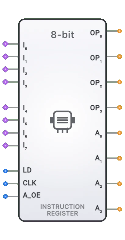
- Instruction Register: Loaded via IR_LD and provides opcode/address splitting
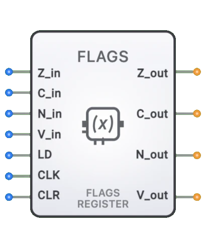
- Flags Register: Updated via FLG_LD and read for conditional jumps (Z_FLAG)
- Accumulator: Controlled via ACC_LD and ACC_OE signals
Signal Timing
The Control Unit ensures proper setup and hold times for all components:
- Address Setup: Address signals are stable before memory operations
- Data Valid: Data is valid when load signals are active
- Clock Synchronization: All state changes occur on clock rising edges
- Reset Behavior: Immediate asynchronous reset to known state
Usage Examples
Simple Program: Add Two Numbers
; Add two numbers stored in memory
0x0: LDA 0x8    ; Load first number from address 0x8
0x1: ADD 0x9    ; Add second number from address 0x9
0x2: STA 0xA    ; Store result at address 0xA
0x3: HLT        ; Halt execution
...
0x8: 0x05       ; First number (5)
0x9: 0x03       ; Second number (3)
0xA: 0x00       ; Result location
Loop Example: Count from 1 to 10
; Count from 0 to 10
0x0: LDA 0x8    ; Load counter
0x1: ADD 0x9    ; Add 1
0x2: STA 0x8    ; Store counter
0x3: SUB 0xA    ; Subtract 10
0x4: JNZ 0x0    ; Jump back if not zero
0x5: HLT        ; Halt when done
...
0x8: 0x00       ; Counter
0x9: 0x01       ; Constant 1
0xA: 0x0A       ; Constant 10
Technical Notes
Clock Requirements
- Minimum Frequency: 1 Hz for educational observation
- Maximum Frequency: Limited by component propagation delays
- Duty Cycle: 50% recommended for optimal timing margins
Reset Behavior
- Asynchronous Reset: Immediately sets state to FETCH
- Signal Clearing: All control signals reset to inactive state
- Halt Recovery: Requires reset to resume execution
Performance
- All Instructions: 4 clock cycles (fetch-decode-execute-store)
- Instructions Per Second: Clock frequency ÷ 4
- Memory Bandwidth: One read or write per instruction cycle