Logic Lab · Templates
Circuit Templates
Explore digital logic circuits covering gates, arithmetic, storage, counters, memory, and processor datapaths
Featured Templates
Selected circuits spanning foundational and more advanced digital logic topics
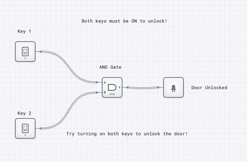
Two-Key AND Gate Demonstration
Two switches feed a 2-input AND gate, and the output light is HIGH only when both inputs are HIGH. The security framing is an educational Boolean model, not a deployable access-control system.Open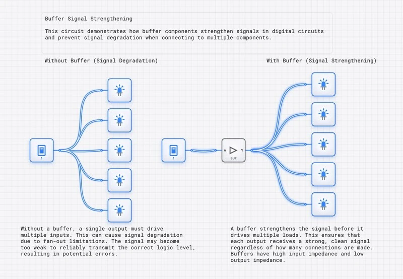
Buffer Fan-Out Demonstration
Compares direct and buffered five-load fan-out at the Boolean level. It demonstrates non-inverting buffer placement but does not model drive strength, capacitance or timing.Open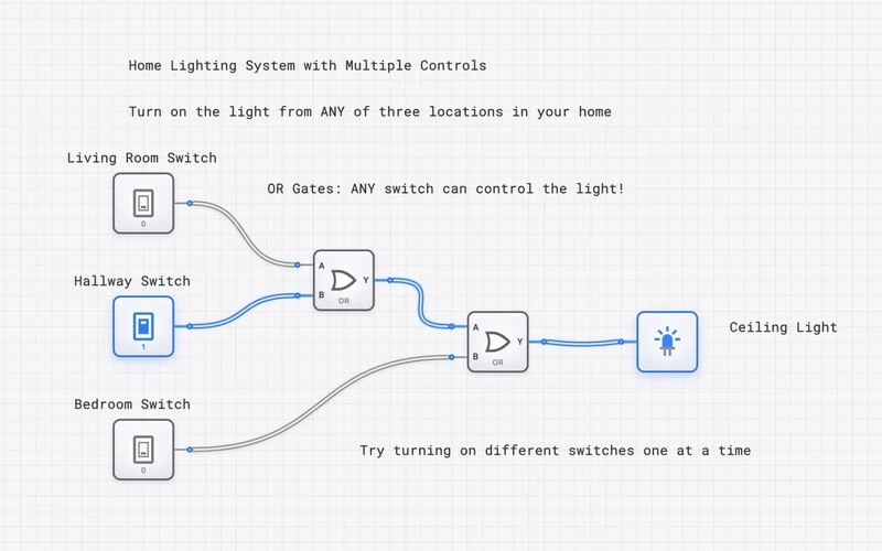
Three-Switch OR Gate Lighting Circuit
Two cascaded OR gates combine three maintained switch signals into one light-control request. This is request aggregation, not the traveler wiring used by residential multiway switches.Open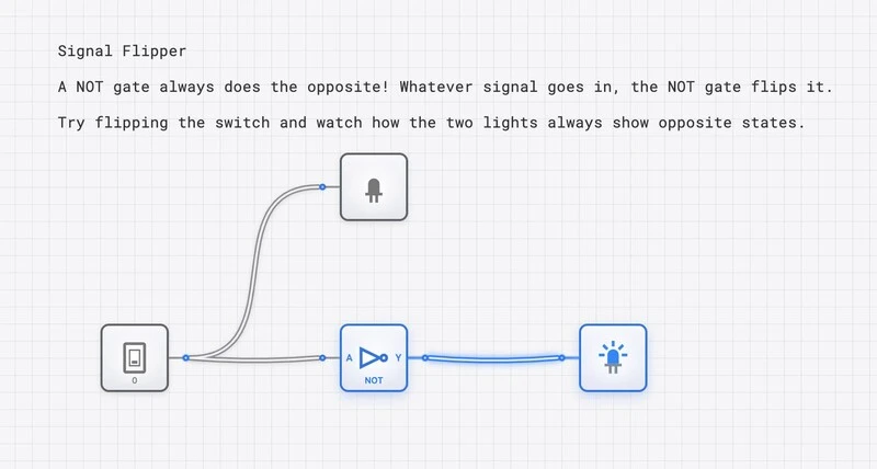
NOT Gate Dual-Output Inverter
A switch drives one light directly and a second through a NOT gate. The two visible outputs are complementary for either binary input state.Open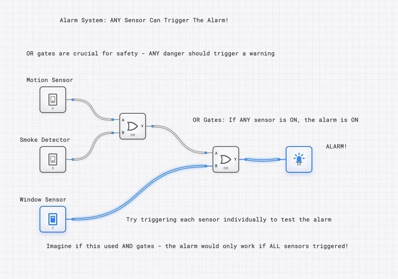
Three-Sensor OR Gate Alarm Logic
Two cascaded OR gates assert one alarm indicator when any of three maintained sensor inputs is HIGH. The circuit omits sensor physics, latching, acknowledgment, diagnostics, and fail-safe output hardware.Open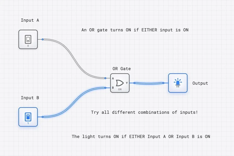
2-Input OR Gate
Two switches drive an inclusive OR gate and one output light. The output is LOW only for 00 and HIGH for the other three binary input combinations.OpenLogic Fundamentals
2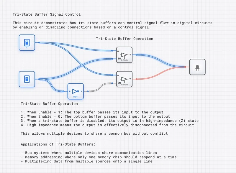
Complementary Tri-State Buffers
Two tri-state buffers receive the same data bit and use complementary enables on one shared node. For either binary enable value, exactly one branch drives, so the visible output always equals the data input and never exposes an all-disabled state.Open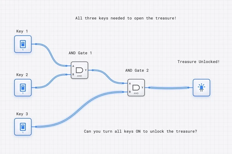
Three-Input Cascaded AND Gate
Two cascaded 2-input AND gates implement a three-input conjunction. The output is HIGH only for input 111, while the unequal gate depths remain visible in the topology.OpenDerived Gates
6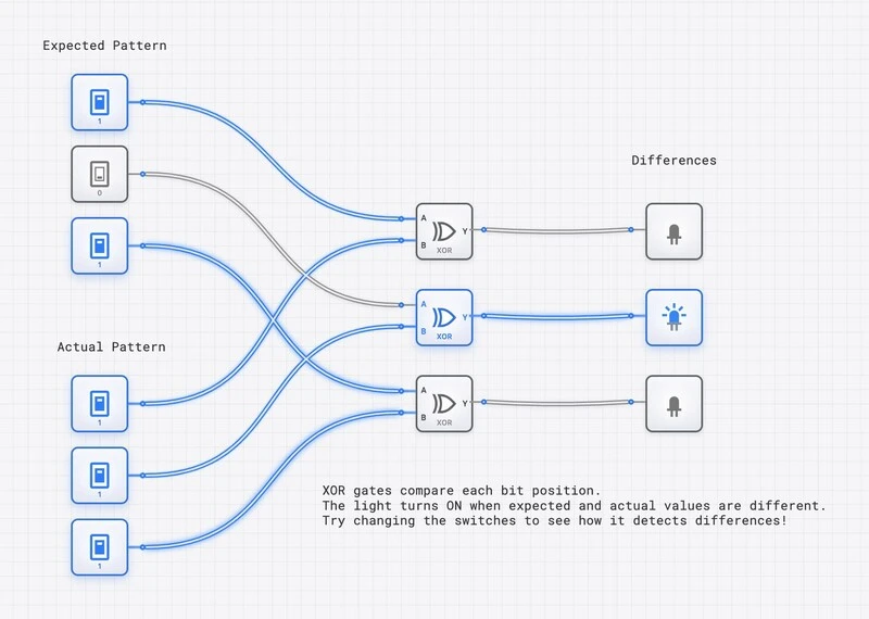
3-Bit XOR Difference Mask
Three parallel XOR gates compare two 3-bit words and expose a bitwise mismatch mask on three lights. The circuit has no oscilloscope and does not reduce the mask to a single equality or any-difference output.Open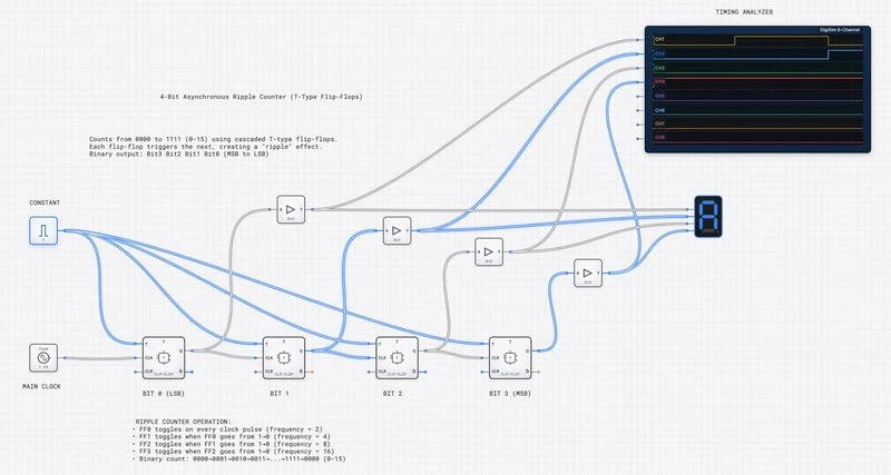
4-Bit Asynchronous Ripple Down-Counter
Four rising-edge T flip-flops are clocked from the preceding Q outputs, producing a modulo-16 down-count when Q0 is interpreted as the least-significant bit. The display and scope show digital states, not device-level ripple timing.Open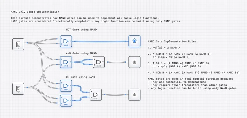
NAND-Only NOT, AND, and OR
Six NAND gates implement NOT A, A AND B, and A OR B as three visible functions. The circuit demonstrates functional completeness through explicit gate-level transformations.Open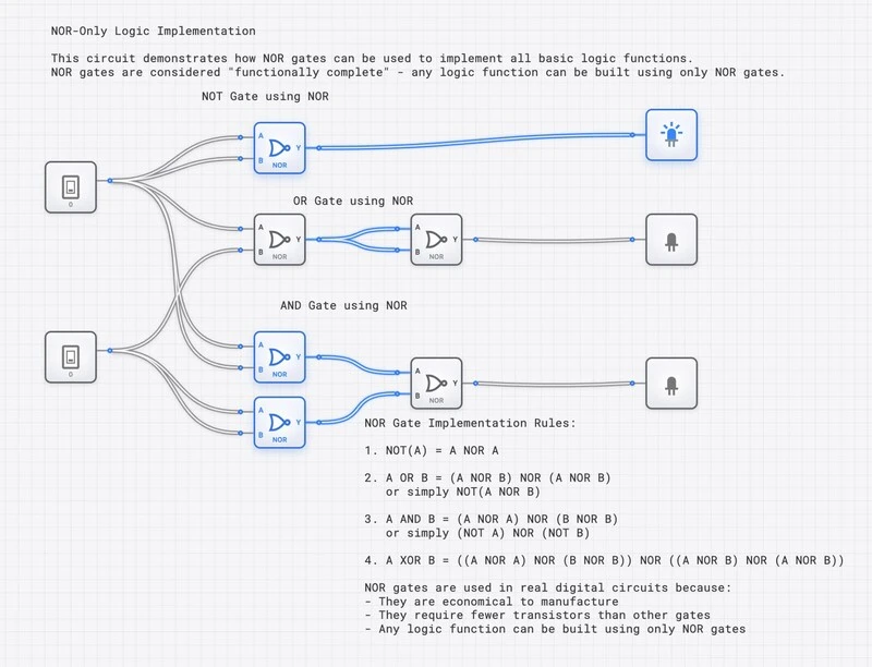
NOR-Only NOT, OR, and AND
Six NOR gates implement NOT A, A OR B, and A AND B as three visible functions. The circuit demonstrates functional completeness through explicit gate-level transformations.Open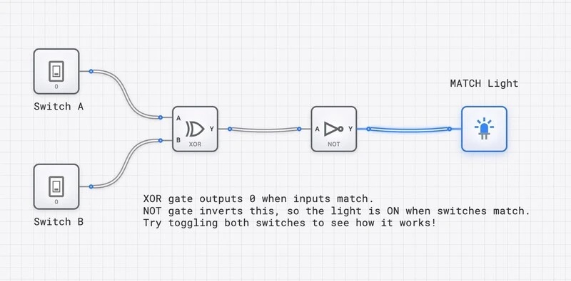
Single-Bit Equality Detector
An XOR gate forms an internal difference signal and a NOT gate converts it to the visible MATCH output. The light is HIGH for 00 and 11, which is the XNOR equality function.Open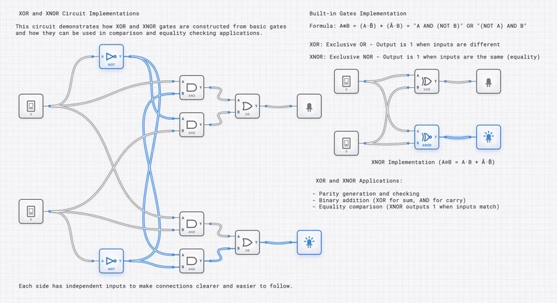
XOR and XNOR Gate-Level Comparison
Gate-level networks are compared with packaged XOR and XNOR components across two independent input pairs. The visible outputs distinguish equality from difference without implying identical physical implementations.OpenCombinational Logic
27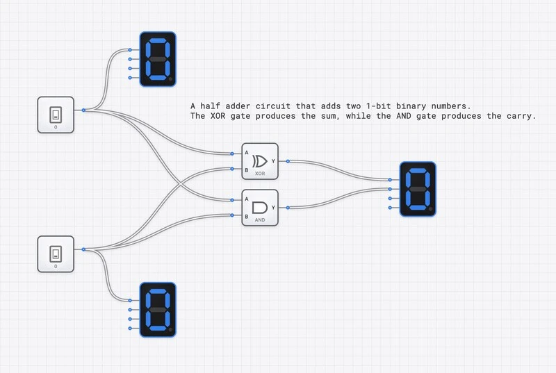
1-Bit Half Adder
An XOR gate produces Sum and an AND gate produces Carry for two one-bit operands. Three digit displays show the operands and the combined two-bit result.Open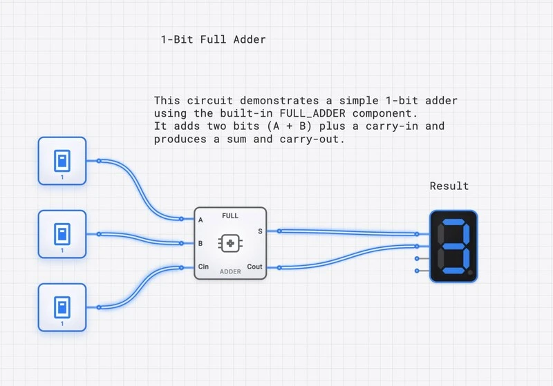
1-Bit Packaged Full Adder
One FULL_ADDER component adds A, B, and Cin. Its digit display combines Sum and Cout into the two-bit arithmetic result.Open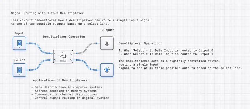
1-to-2 Demultiplexer
One select bit routes data input D to Y0 or Y1 while driving the unselected output LOW. When D is LOW, both visible outputs are LOW.Open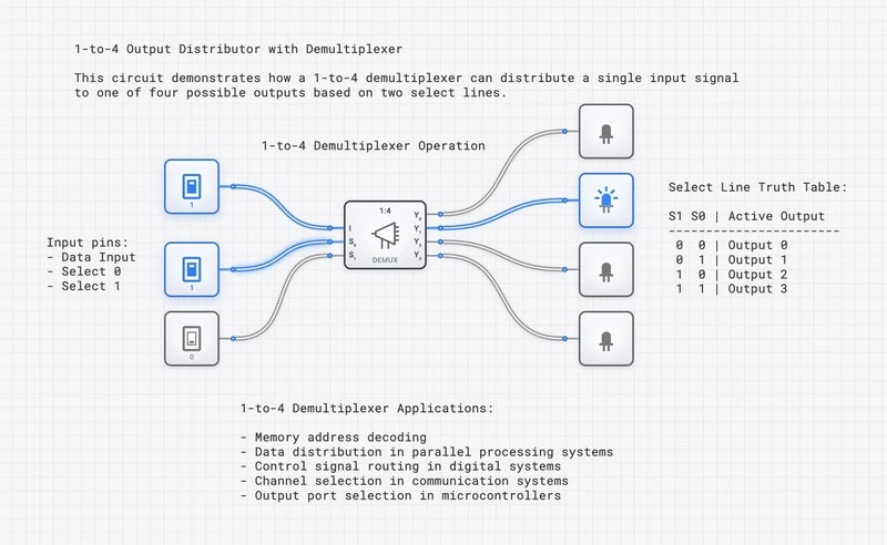
1-to-4 Demultiplexer
A 2-bit select code routes one data input to one of four outputs. The selected output follows D, and the other three outputs remain LOW.Open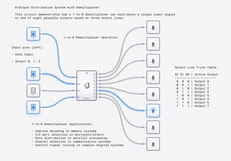
1-to-8 Demultiplexer
A 3-bit select code routes one data input to one of eight outputs. With D HIGH the output vector is one-hot; with D LOW all eight outputs are LOW.Open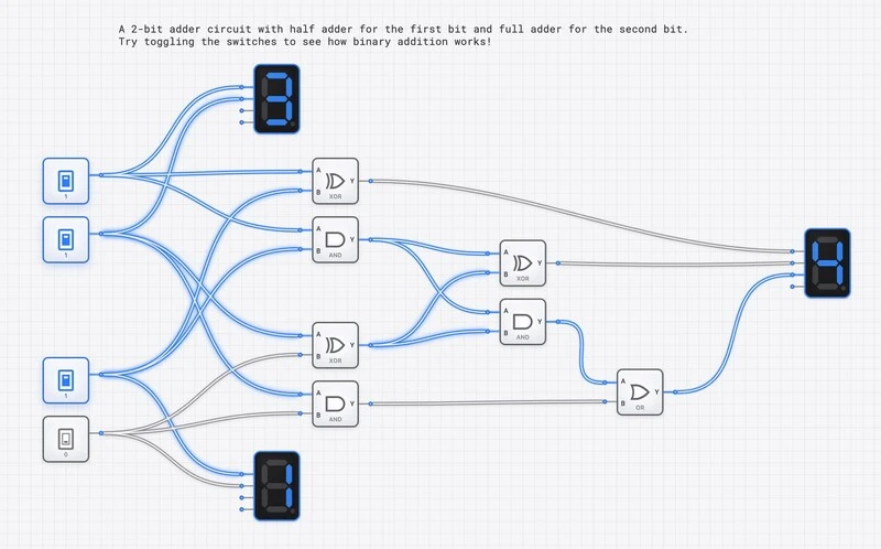
2-Bit Binary Adder
Individual XOR, AND, and OR gates add two 2-bit unsigned operands. The least-significant half-adder stage feeds a full-adder network, and a digit display shows the three-bit result.Open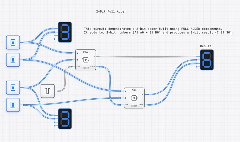
2-Bit Full-Adder Chain
Two packaged full adders form a 2-bit ripple-carry path with the first carry-in fixed LOW. Three digit displays show both operands and the three-bit result.Open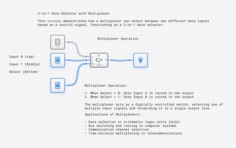
2-to-1 Multiplexer
One select bit chooses whether output Y follows D0 or D1. The packaged component implements Y = (NOT S AND D0) OR (S AND D1).Open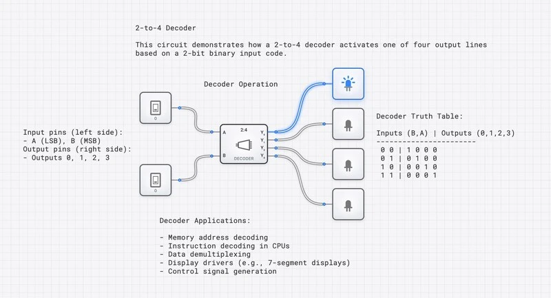
2-to-4 Decoder
A 2-bit input code asserts exactly one of four active-HIGH outputs. The circuit exposes the four one-hot decode states directly on output lights.Open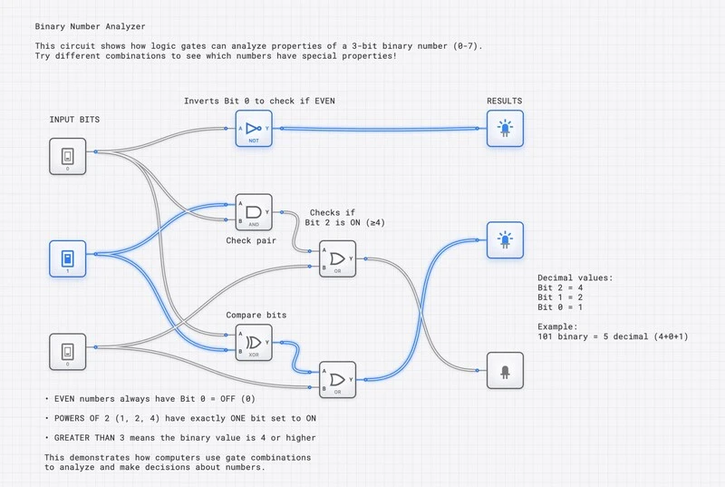
3-Bit Binary Number Analyzer
Three independent gate networks report even values, B2 OR (B1 XOR B0), and values at least 3. These functions follow the executable wiring, including places where canvas annotations are inconsistent.Open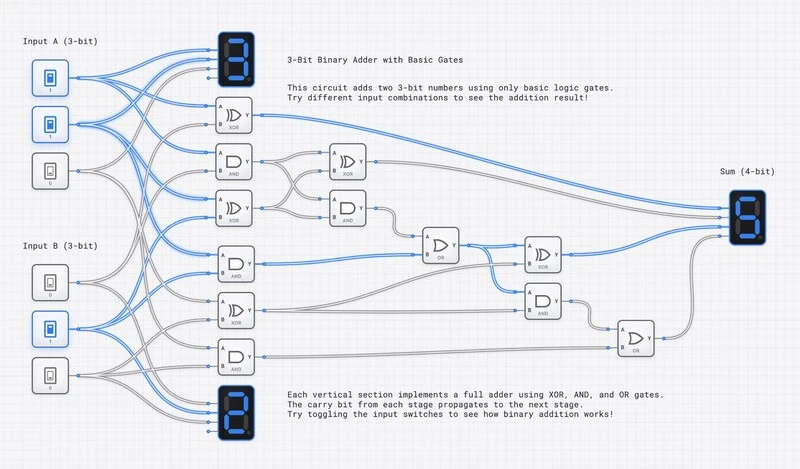
3-Bit Gate-Level Binary Adder
Five XOR gates, five AND gates, and two OR gates form a 3-bit ripple-carry adder without packaged full-adder components. The result display receives the three sum bits and final carry.Open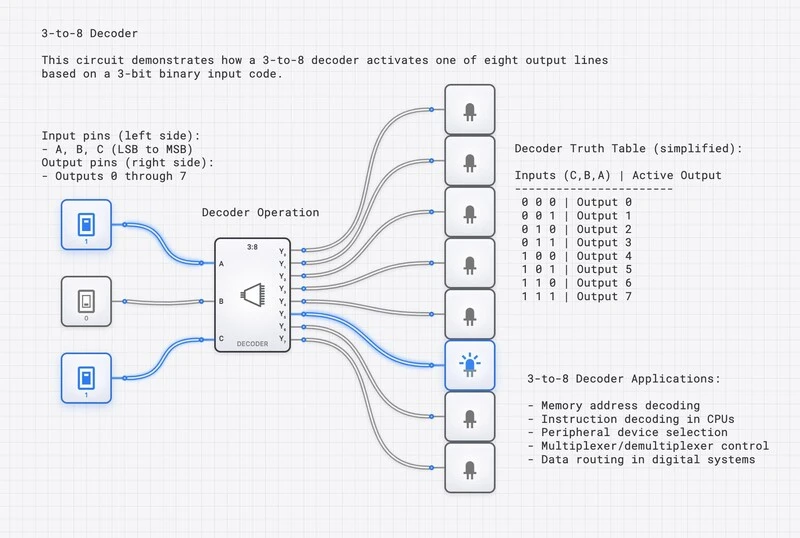
3-to-8 Decoder
A 3-bit input code asserts exactly one of eight active-HIGH outputs. Each output corresponds to one three-variable minterm.Open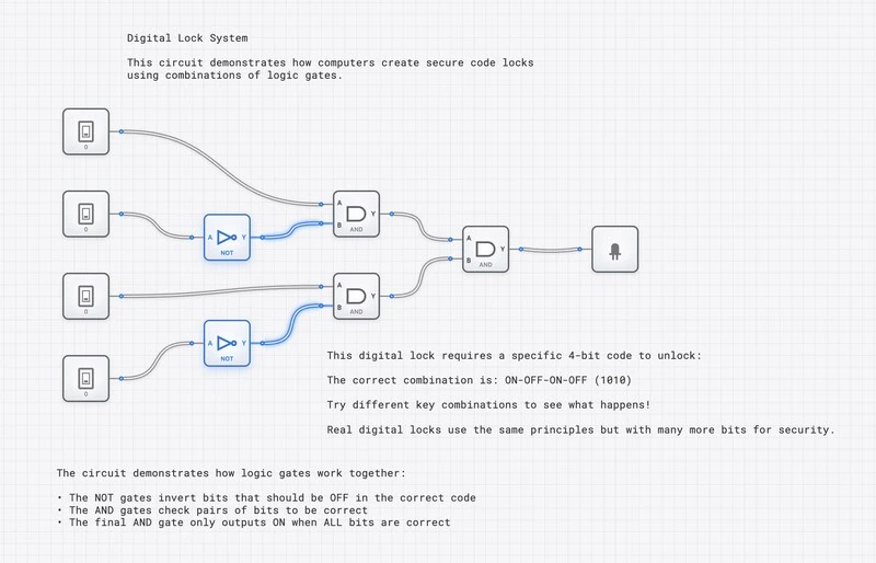
4-Bit Code Detector (1010)
NOT and AND gates implement the minterm that asserts the output only for input 1010. The visible code and purely combinational output make this a decoder example, not a secure authentication mechanism.Open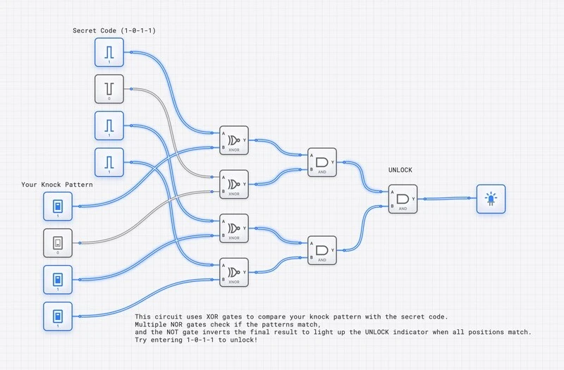
4-Bit Combination Lock (1011)
Four XNOR comparisons and a two-level AND tree assert the output only when the switch word equals the stored reference 1011. One disconnected HIGH constant is present but cannot affect the result.Open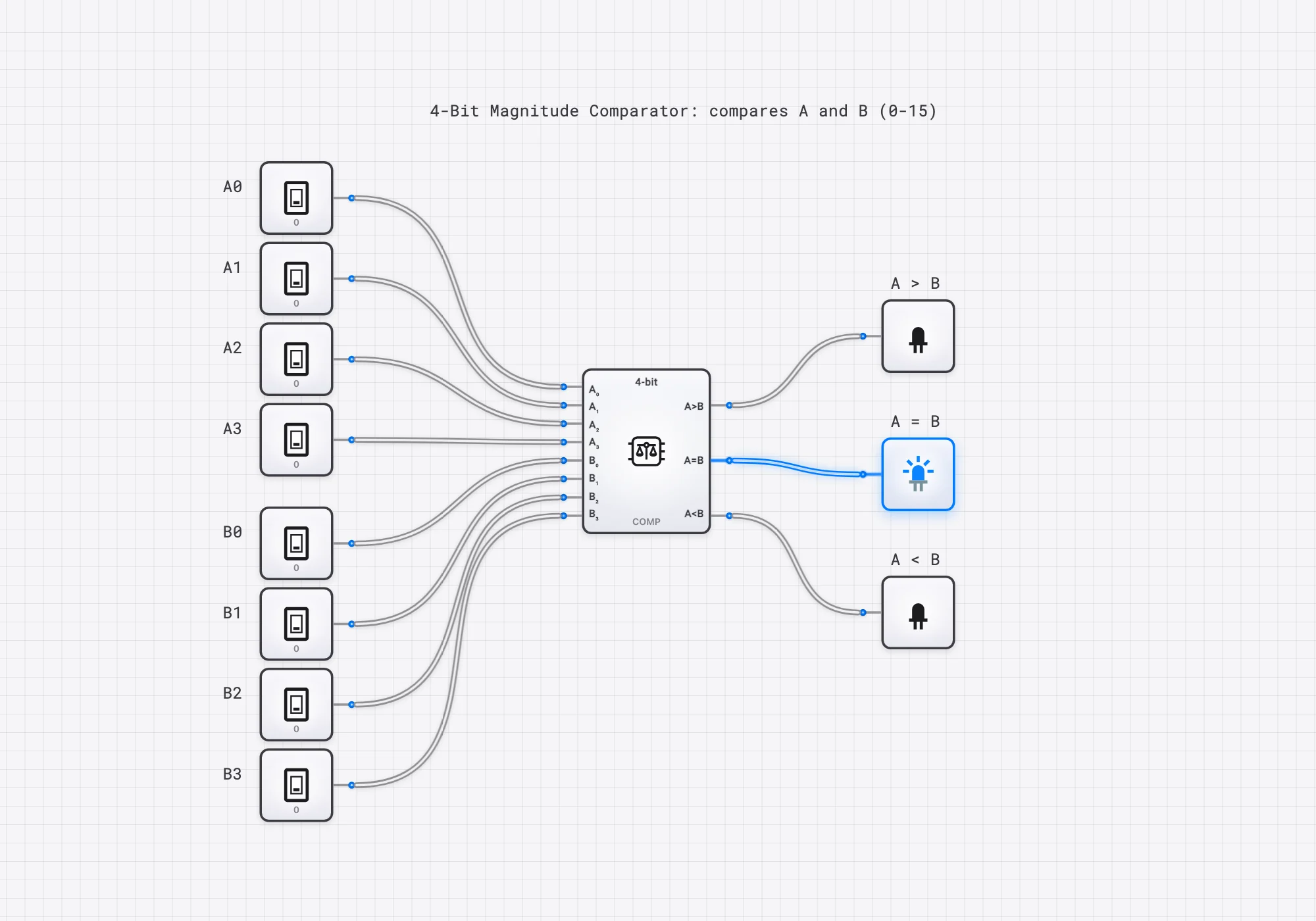
4-Bit Magnitude Comparator
Eight switches define unsigned operands A and B, and three mutually exclusive lights report A greater than B, A equal to B, or A less than B. Production runtime identity 126 resolves to canonical content identity 125 for this same reviewed circuit.Open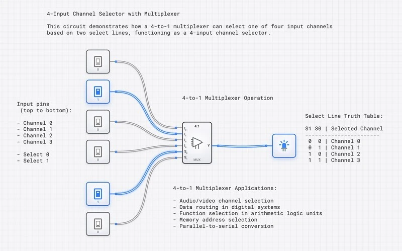
4-to-1 Multiplexer
A 2-bit select code routes one of four data inputs to a single output. Changing an unselected data input does not affect the output.Open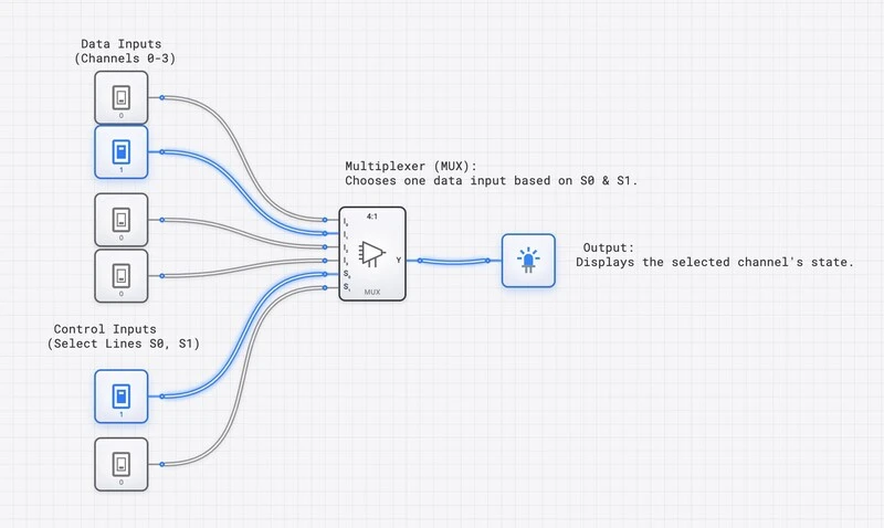
4-to-1 MUX Channel Selector
A 2-bit select code routes one of four single-bit channel inputs to the output. The television framing is a data-selection metaphor; it does not model an audio or video signal path.Open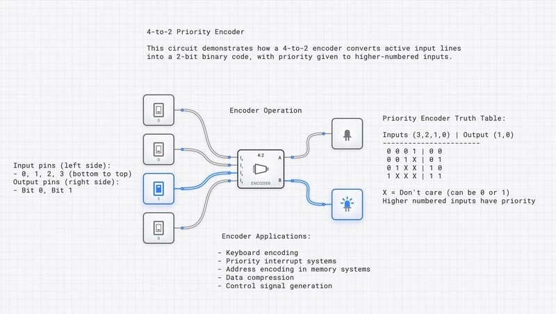
4-to-2 Priority Encoder
Maps the highest-priority asserted input among four lines to a 2-bit binary index. The displayed circuit has no valid output, so I0 and no active input both appear as 00.Open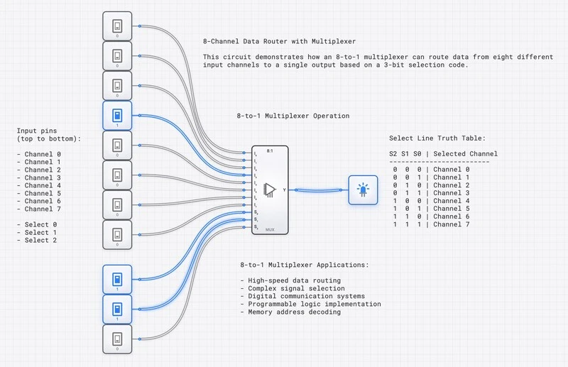
8-to-1 Multiplexer
A 3-bit select code routes one of eight data inputs to a single output. The selected input follows the binary index S2S1S0.Open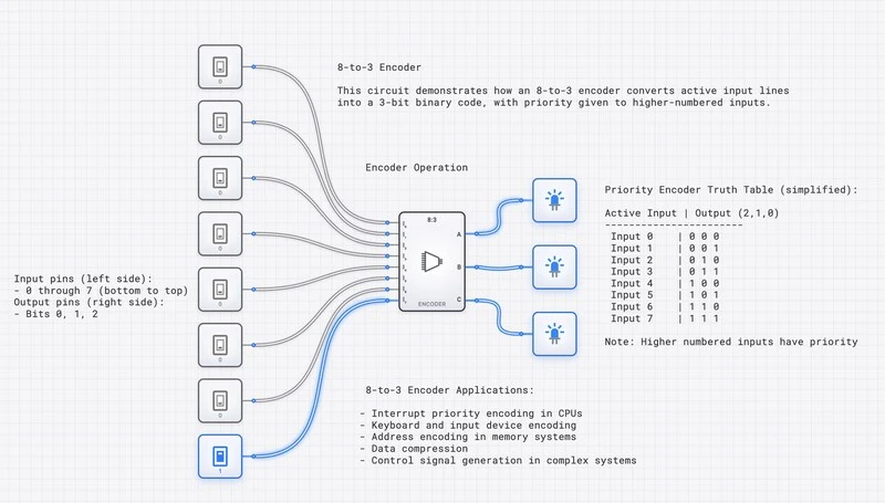
8-to-3 Priority Encoder
Maps the highest-priority asserted input among eight lines to a 3-bit binary index. The displayed circuit has no valid output, so I0 and no active input both appear as 000.Open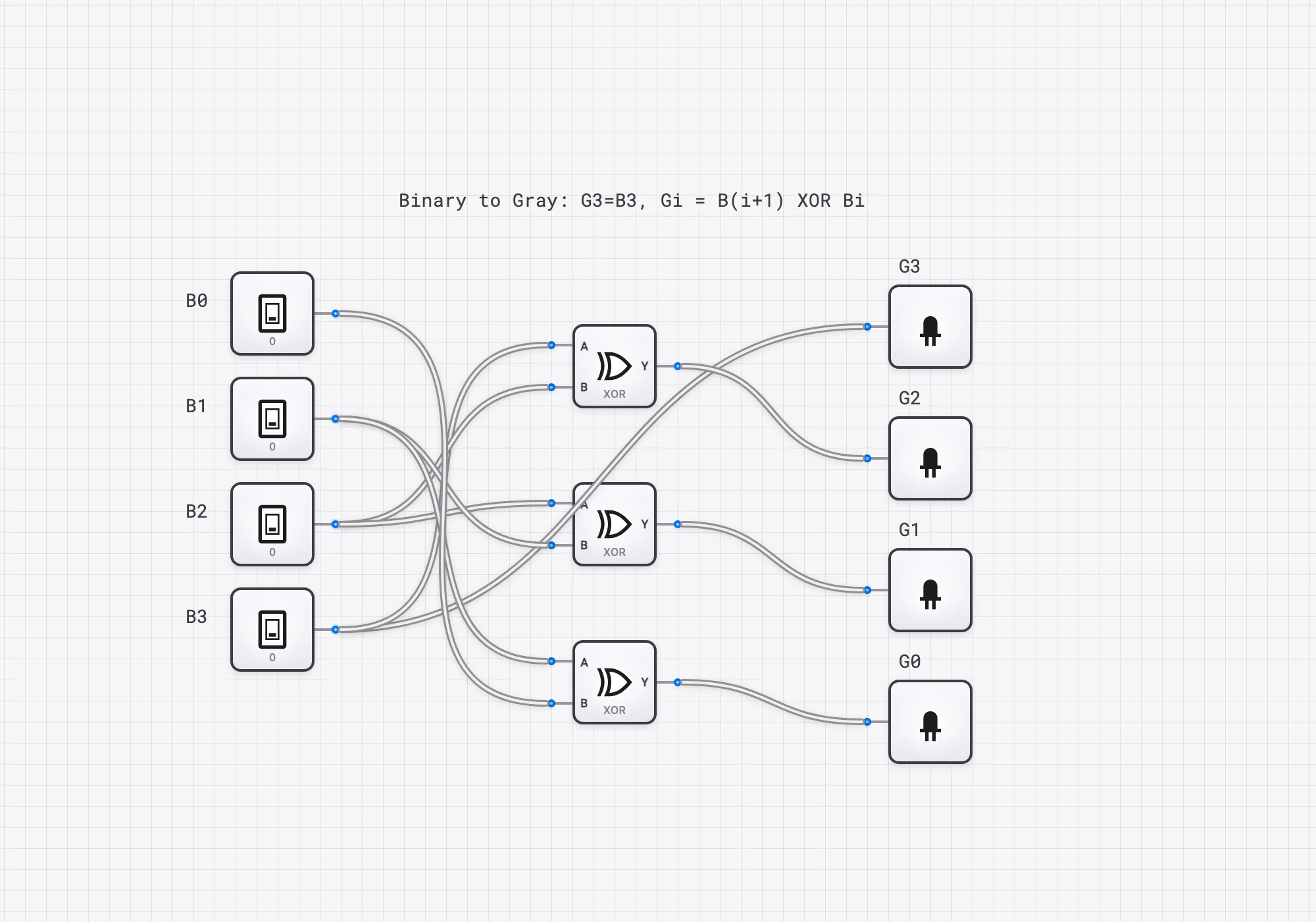
Binary to Gray Code Converter
The most-significant Gray bit copies the binary MSB, while the other three Gray bits XOR adjacent binary inputs. The resulting reflected Gray-code sequence changes one bit between adjacent integer values.Open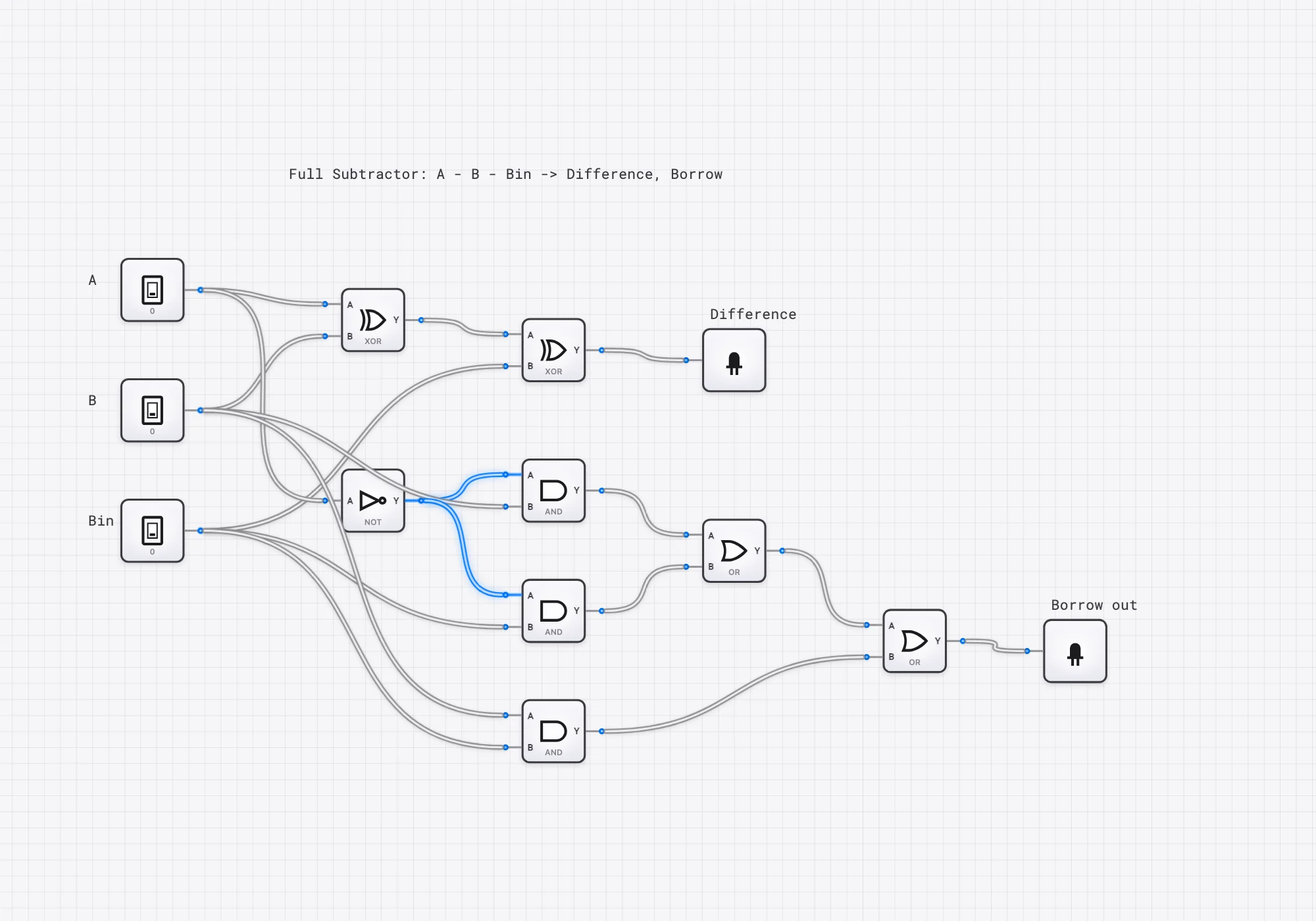
Full Subtractor
Two XOR gates compute Difference for A, B, and Borrow-in, while a three-product network computes Borrow-out. Cascading Borrow-out into the next stage forms a multi-bit ripple-borrow subtractor.Open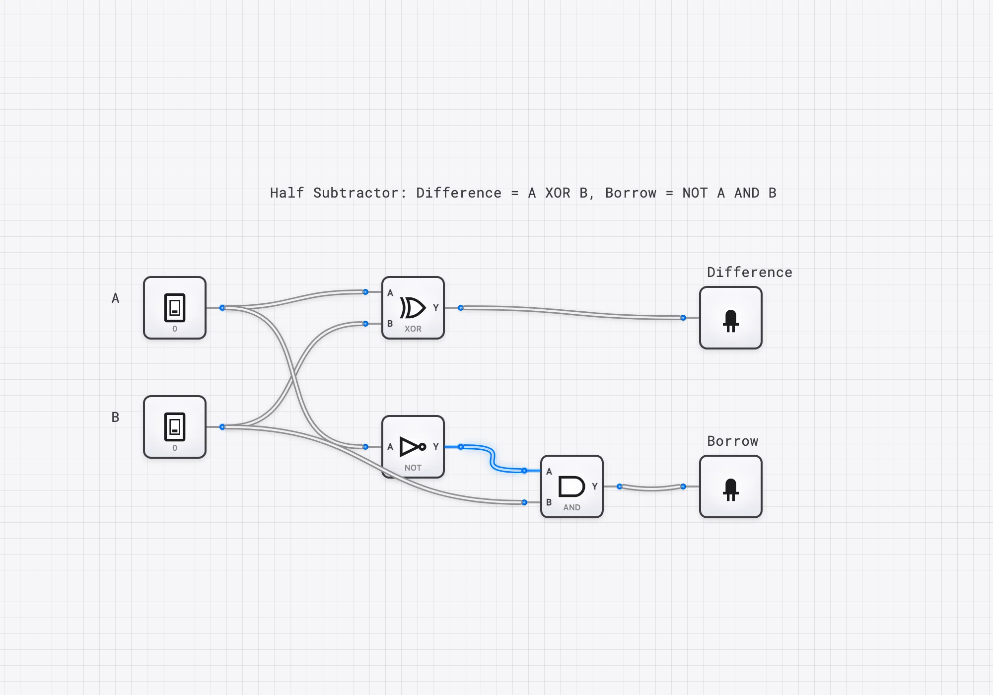
Half Subtractor
An XOR gate computes Difference for A minus B, while NOT A followed by AND with B computes Borrow. The circuit has no Borrow-in and is suitable for the least-significant stage of a larger subtractor.Open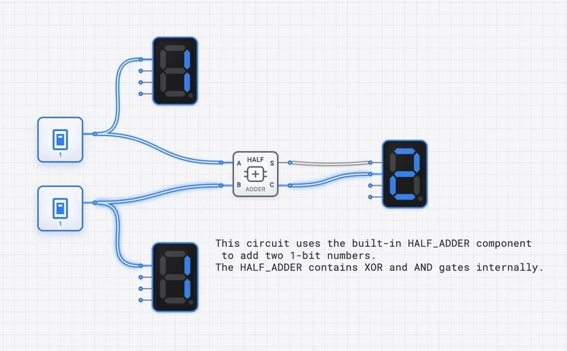
Packaged Half-Adder Demonstration
One HALF_ADDER component computes Sum and Carry from two one-bit operands. Separate digit displays show A, B, and the combined two-bit result.Open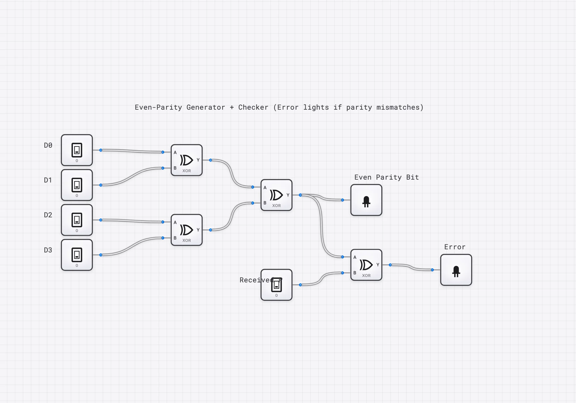
Parity Generator and Checker
An XOR tree generates the even-parity bit for four data bits, and a final XOR compares it with a received parity bit. The checker detects any odd number of bit inversions but cannot locate an error or detect every even-numbered error pattern.Open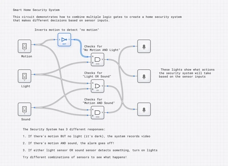
Three-Sensor Multi-Output Logic
Three sensor switches feed three independent combinational functions: Motion AND Sound, NOT Motion AND Light, and Light OR Sound. The graph implements parallel Boolean outputs, not autonomous decision-making.Open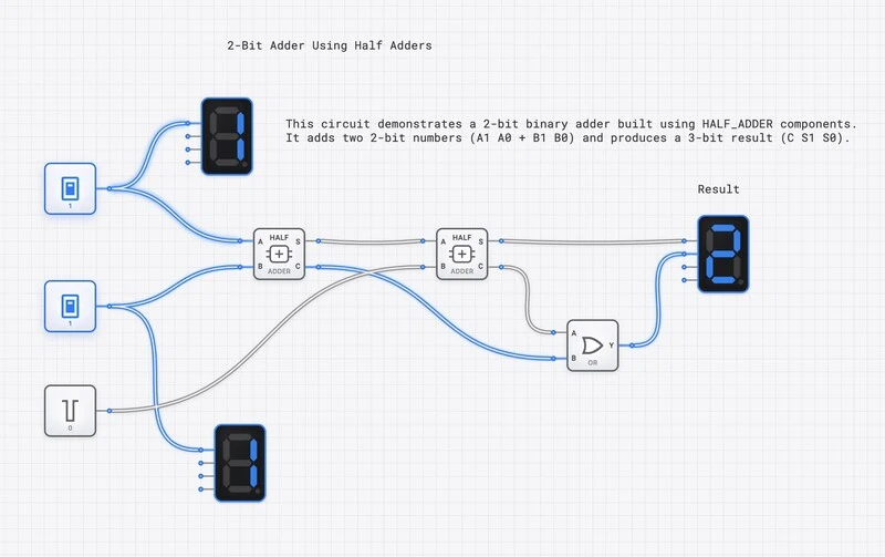
Two-Half-Adder Topology (Cin = 0)
Two half adders and an OR gate resemble a full-adder decomposition, but the second half adder receives a fixed logic 0 instead of a controllable Cin. The external two-input function is therefore a half adder.OpenOutput & Display
3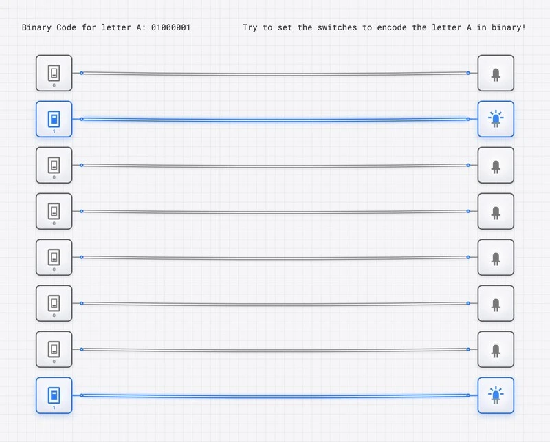
8-Bit Switch and Light Panel
Eight independent switches drive eight corresponding lights with no intervening logic. The suggested 01000001 pattern represents uppercase A only when the bits are interpreted as ASCII.Open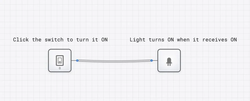
Basic Switch and Light
One switch drives one output light directly, so the displayed logic level equals the input. The circuit models Boolean connectivity, not voltage, current, or loading.Open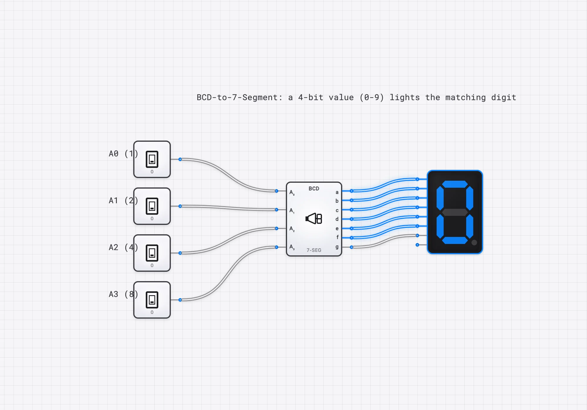
BCD-to-7-Segment Display
A decoder maps BCD inputs 0000 through 1001 to active-HIGH segments a through g. In this simulator model, invalid BCD codes 1010 through 1111 drive every segment LOW and leave the display blank.OpenSequential Logic
7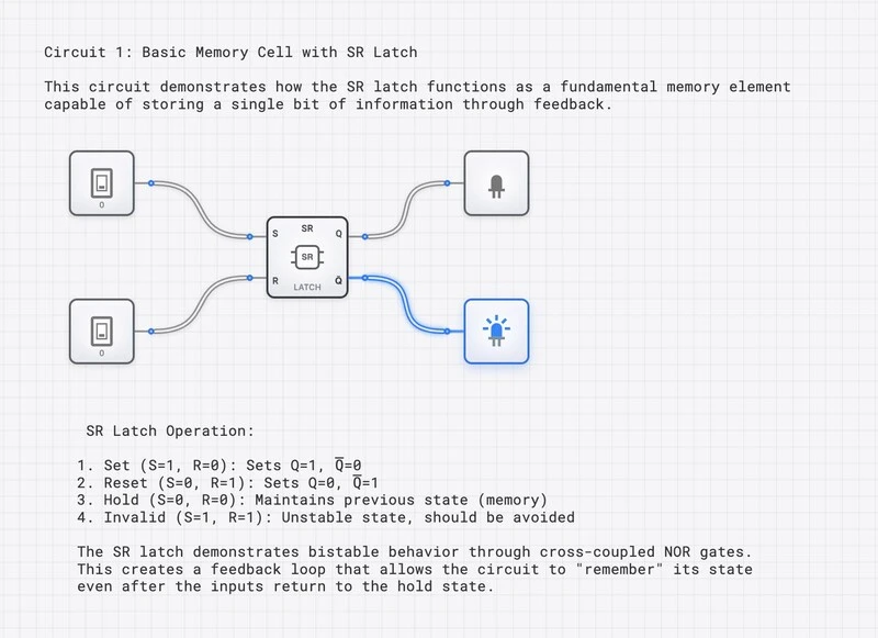
Active-High SR Latch
Set and Reset switches control one packaged active-HIGH SR latch with Q and complementary outputs. The 00 input holds state, 10 sets, 01 resets, and 11 is represented as unknown by this digital model.Open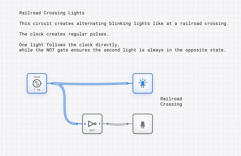
Complementary Clock-Driven Lights
A clock drives one light directly and a second through a NOT gate, producing complementary logic levels. The inverter changes polarity but does not divide frequency, and the circuit contains no storage element.Open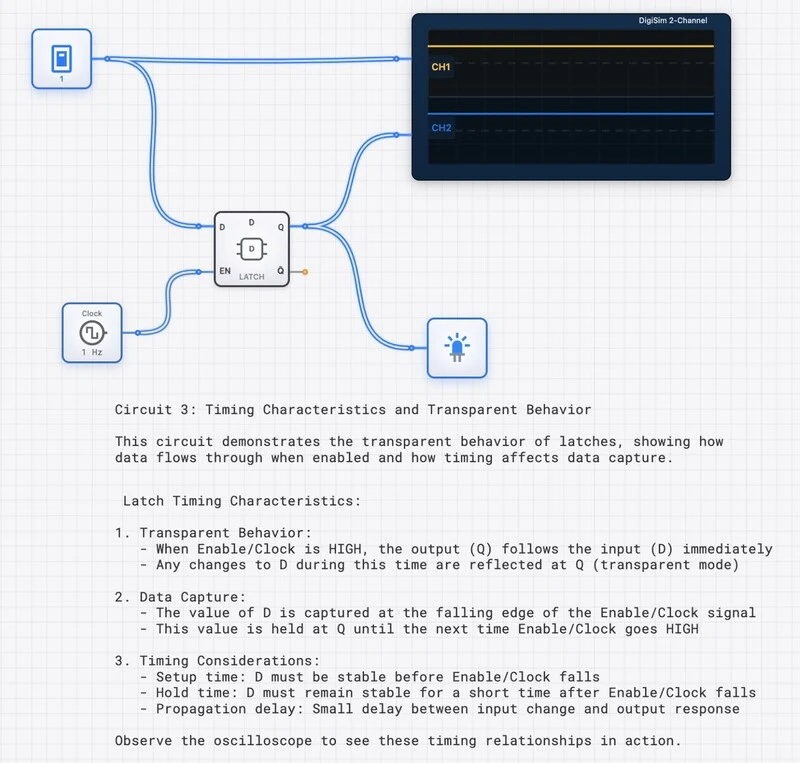
D Latch with Oscilloscope
An oscilloscope displays D and Q while a clock signal drives the latch's active-HIGH enable. The model illustrates transparent and hold intervals but does not characterize setup time, hold time, propagation delay, rise time, or metastability.Open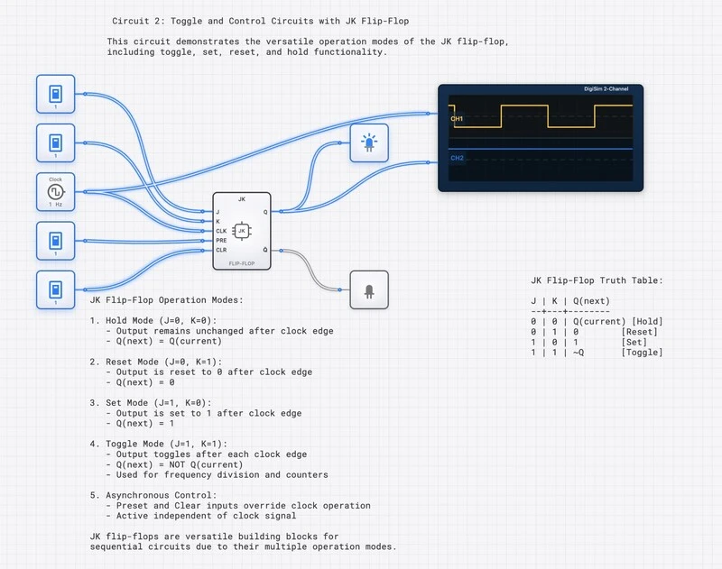
Edge-Triggered JK Flip-Flop
Observe hold, reset, set and toggle behavior at rising clock edges, together with asynchronous preset and clear. The packaged primitive does not expose a master-slave implementation.Open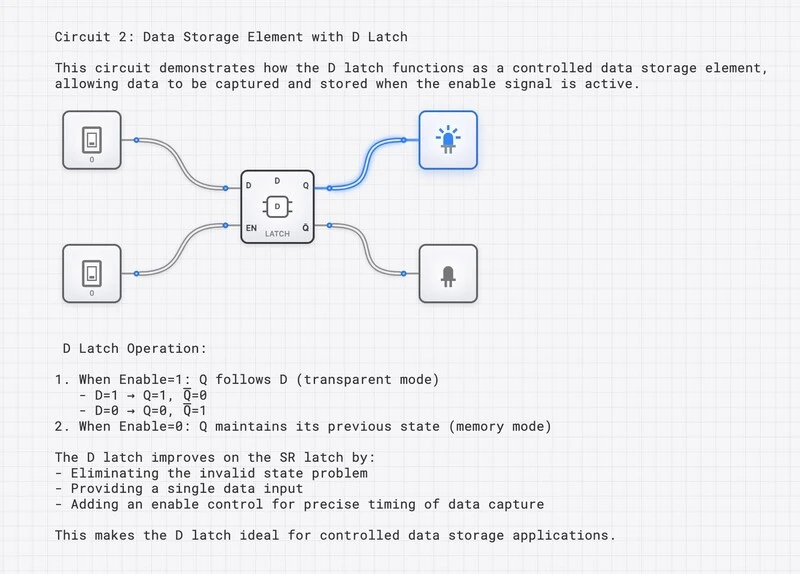
Level-Sensitive D Latch
A packaged D latch follows D while Enable is HIGH and retains the previously accepted bit while Enable is LOW. Two lights expose Q and its complement.Open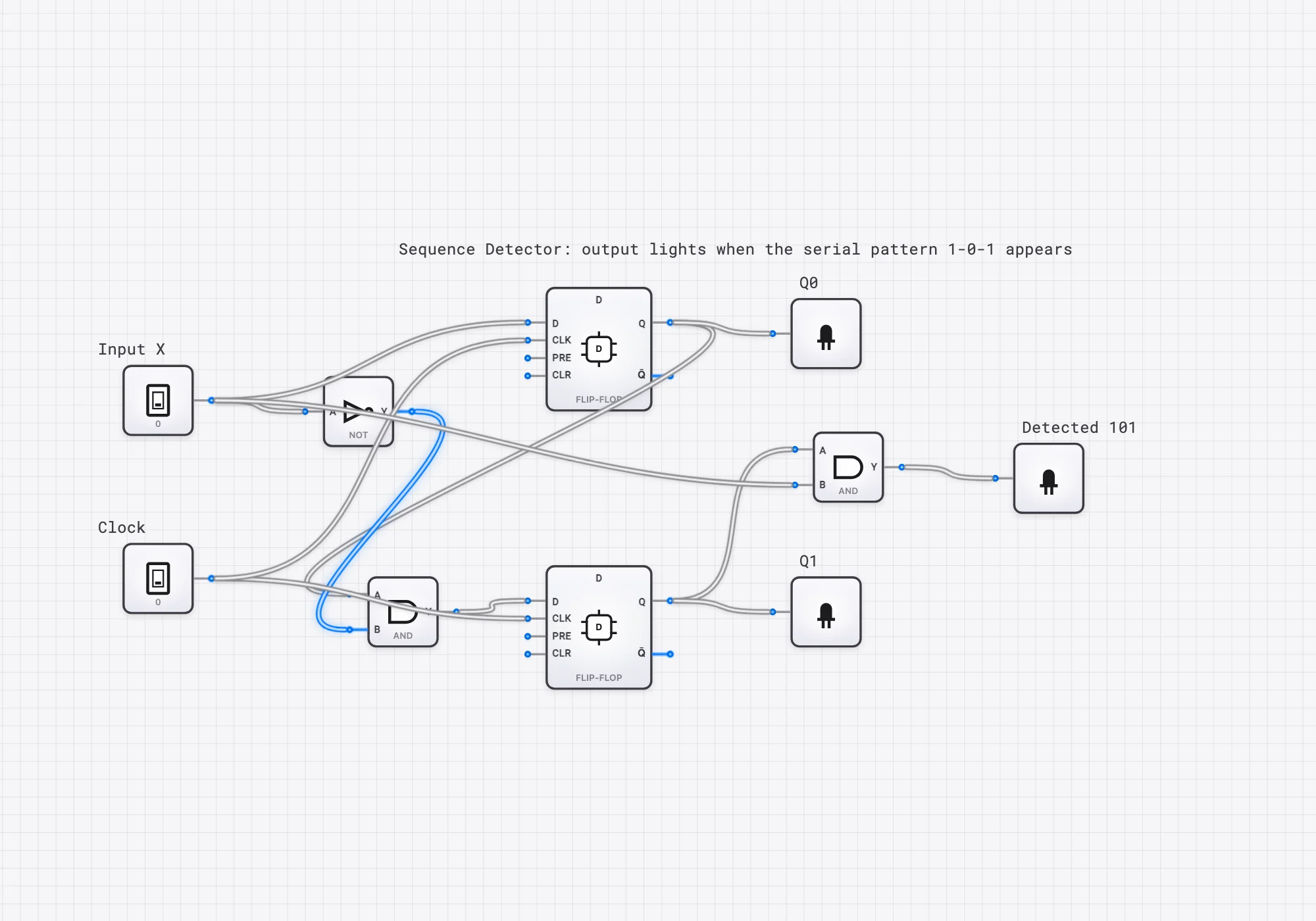
Overlapping 101 Sequence Detector
Two D flip-flops and combinational logic implement a Mealy machine that recognizes overlapping 101 patterns. Because the output depends on current state and current input, it can change between clock edges and requires a defined sampling convention downstream.Open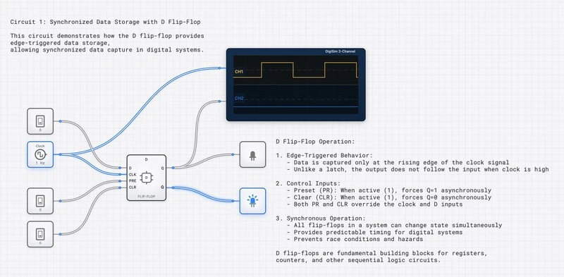
Rising-Edge D Flip-Flop
The flip-flop samples D on rising clock edges and exposes Q and its complement. Active-HIGH preset and clear act asynchronously, with clear taking priority in this simulator model.OpenMemory Systems
18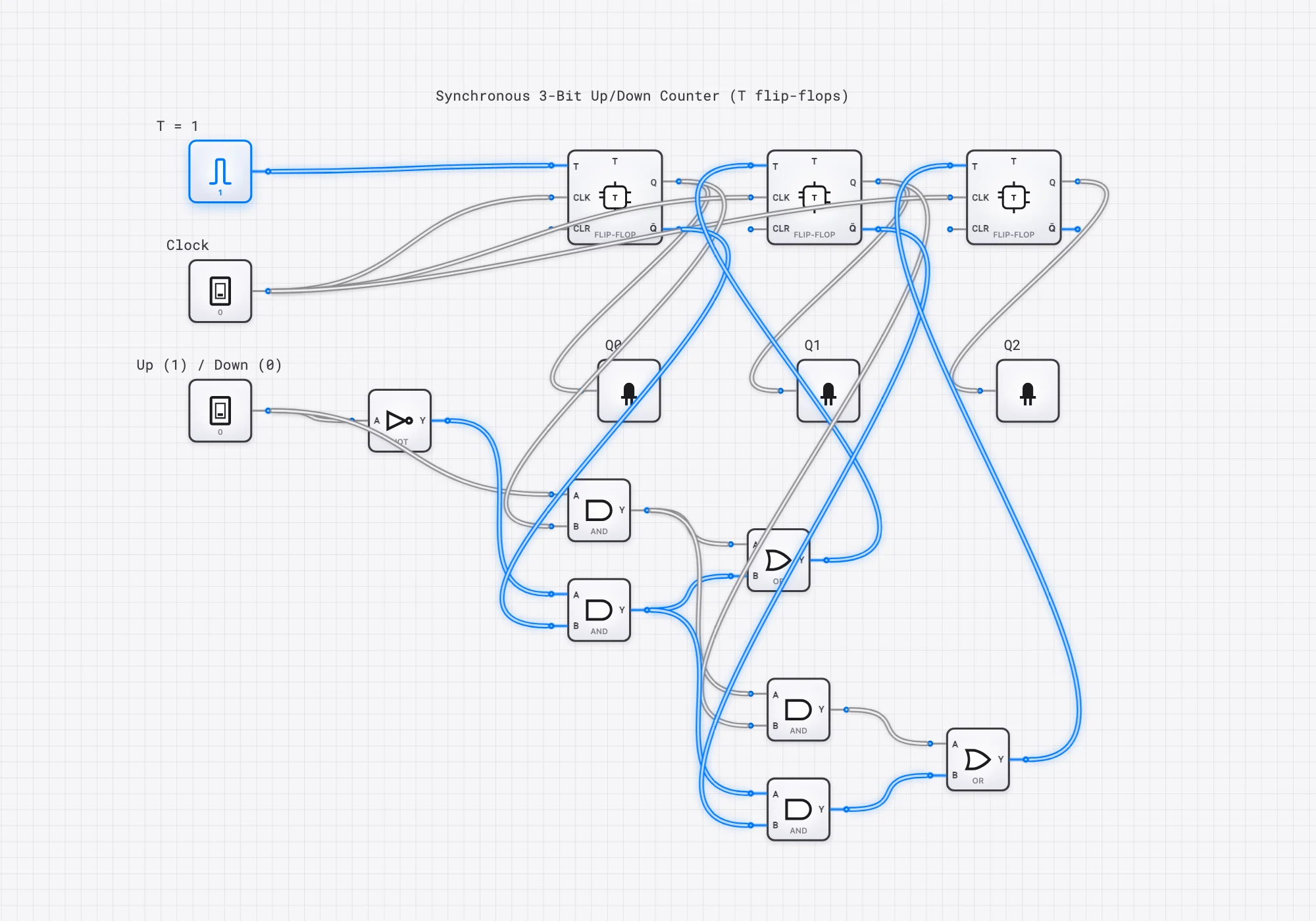
3-Bit Up/Down Counter
A synchronous 3-bit counter that counts up or down depending on a direction input. T flip-flops toggle under combinational steering logic so all bits change on the same clock edge.Open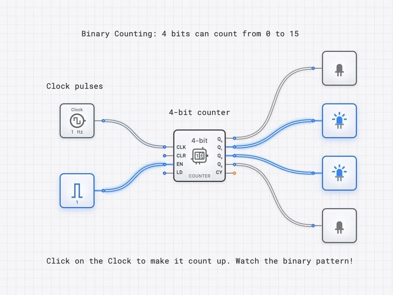
4-Bit Binary Counter
A fixed-HIGH enable lets the packaged 4-bit counter advance modulo 16 on each rising clock edge. Four lights expose Q3..Q0; clear, load, and terminal-count signals are not connected.Open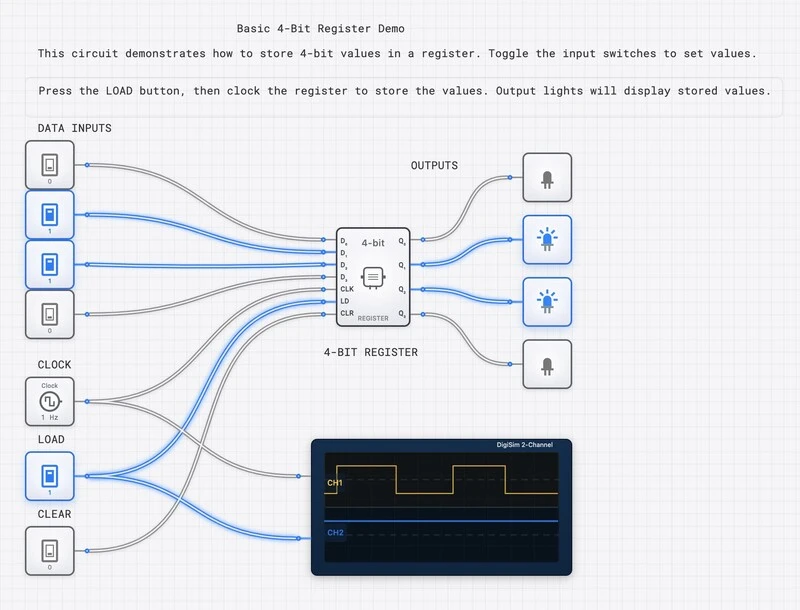
4-Bit Clocked Register
A 4-bit register captures D3..D0 on a rising edge when Load is HIGH and otherwise holds its state. Active-HIGH clear is asynchronous; the scope shows clock and load but does not measure physical timing parameters.Open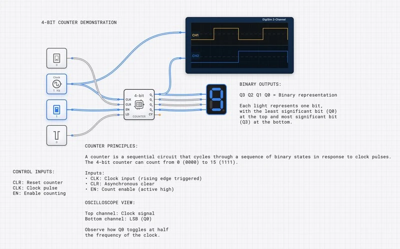
4-Bit Counter with Hexadecimal Display
A 4-bit enabled up-counter advances modulo 16, supports asynchronous clear, and drives one hexadecimal digit display. The two-channel scope observes clock and Q0; the circuit does not contain four output lights or a separate seven-segment display.Open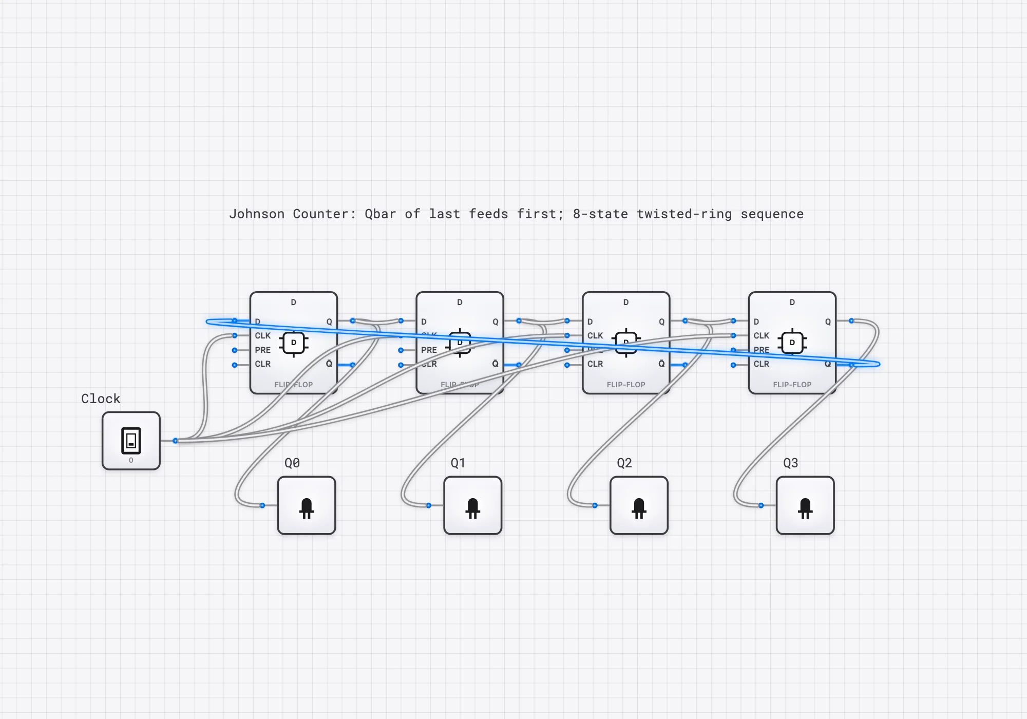
4-Bit Johnson Counter
Four D flip-flops share one clock, with the final complementary output fed back to the first stage. From the simulator's defined 0000 start, the intended Johnson sequence contains eight states; no separate reset control is connected.Open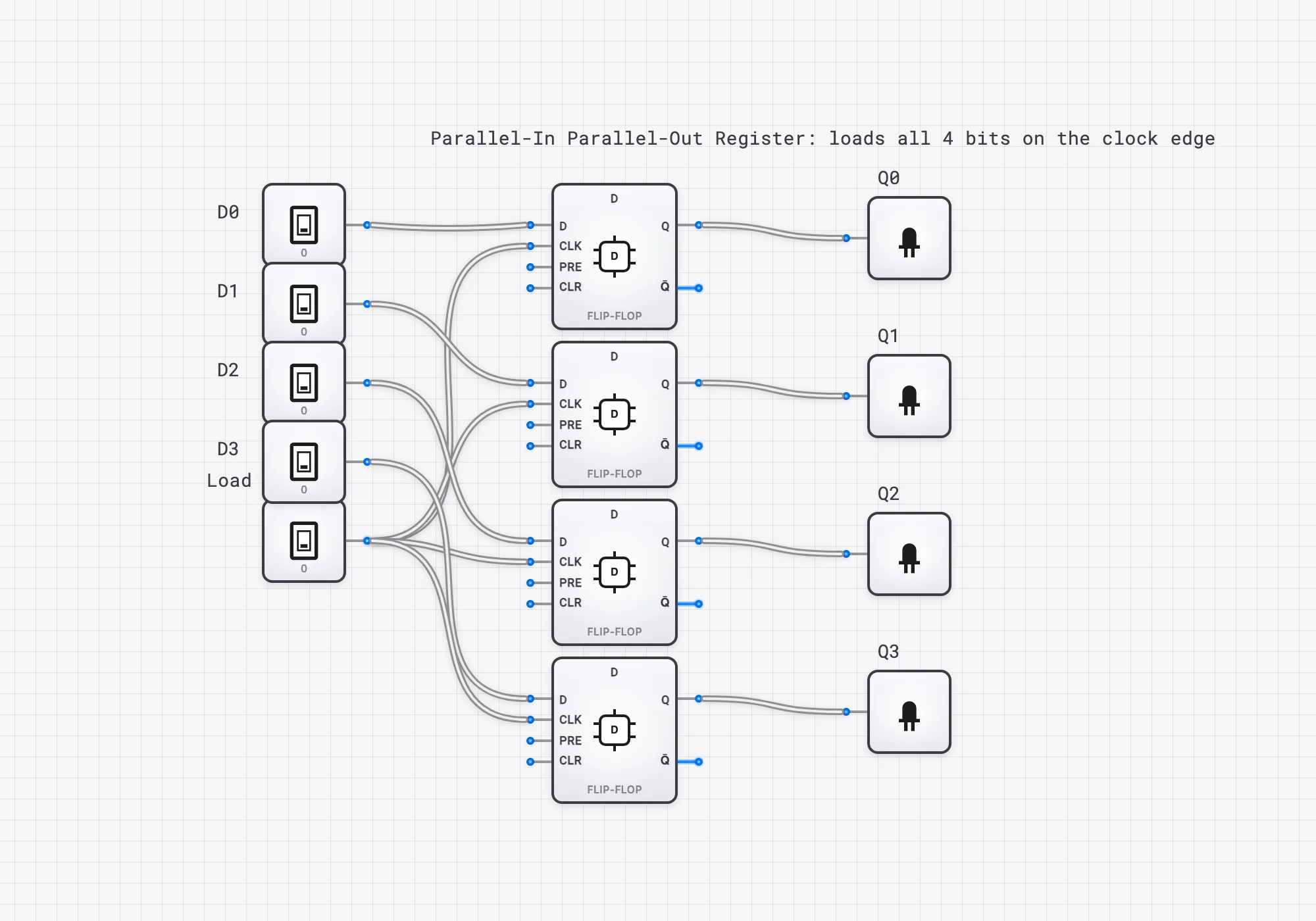
4-Bit PIPO Register
Four D flip-flops sharing a manual clock capture D3..D0 in parallel on a rising edge and retain the word between edges. The ideal digital model demonstrates functional state transitions without specifying physical setup or hold margins.Open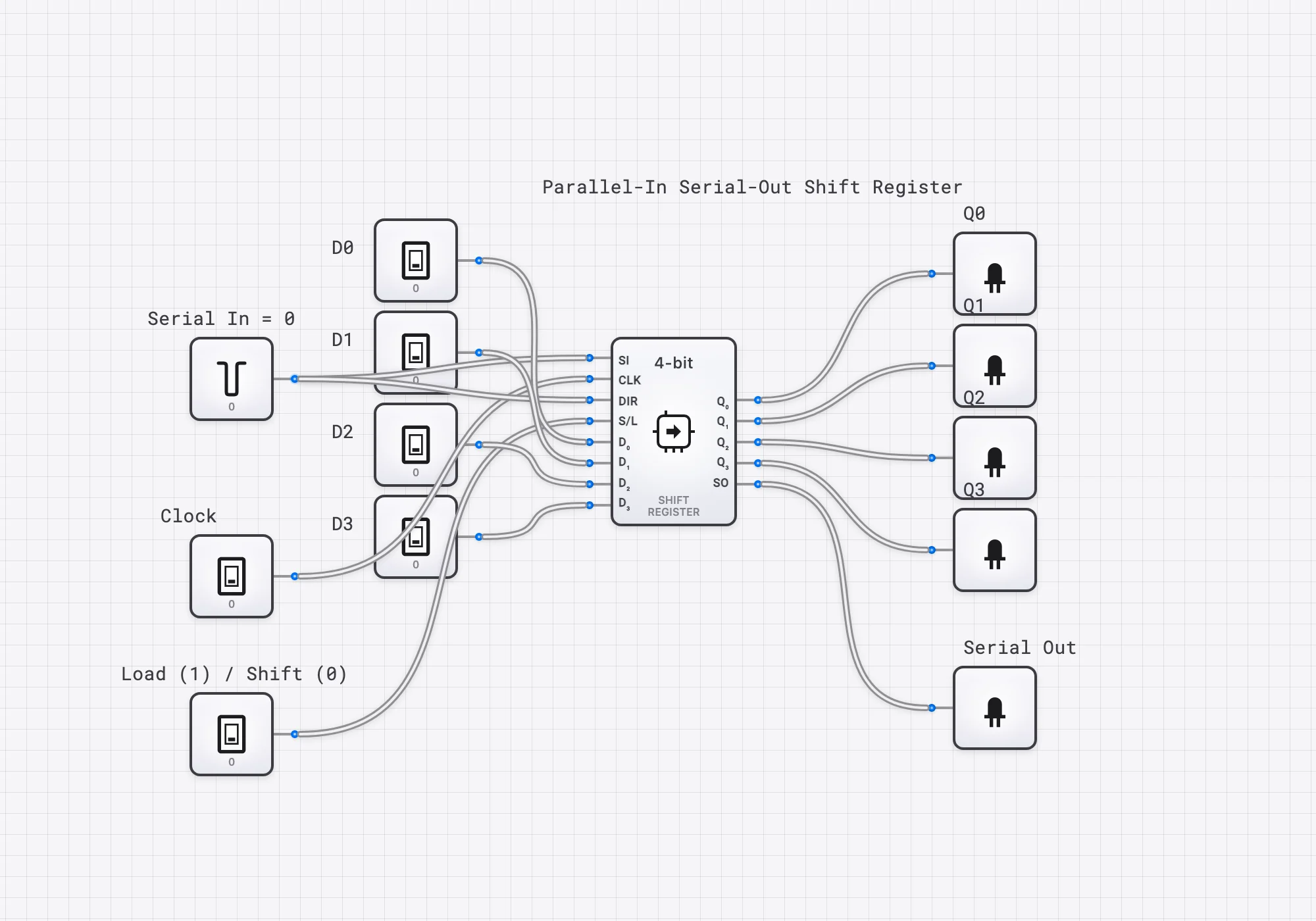
4-Bit PISO Shift Register
Six switches provide D3..D0, a manual clock, and Load/Shift for one packaged register; fixed LOW inputs select right shift and zero fill. After a parallel load, Serial Out presents Q0 first as the stored word shifts toward Q0.Open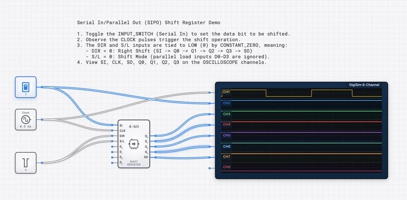
4-Bit Right-Shift Register
Fixed LOW direction and shift/load controls select right-shift mode: SI enters Q3, stored bits move toward Q0, and SO reflects Q0. The scope exposes clock, SI, every Q stage, and SO.Open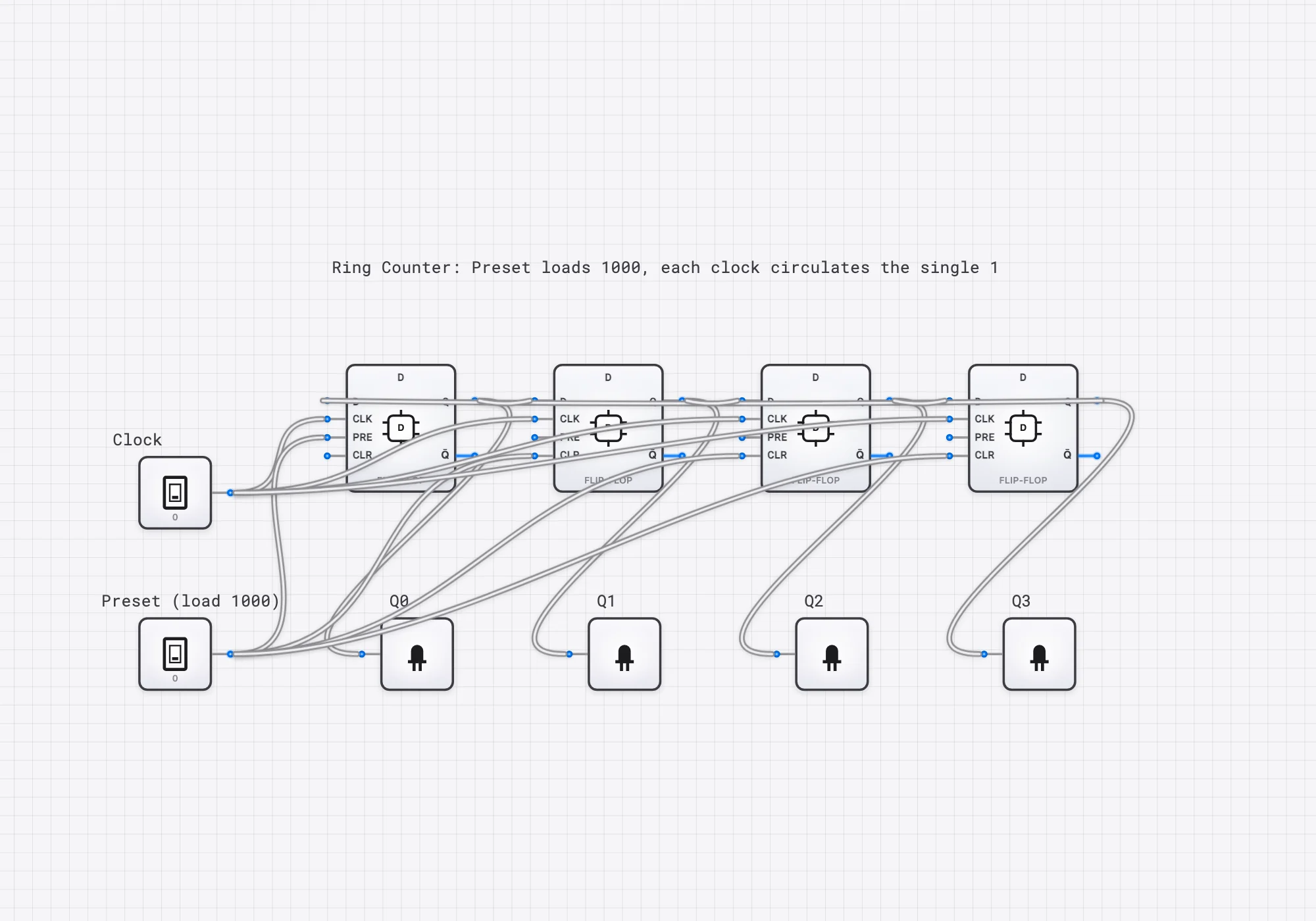
4-Bit Ring Counter
Four D flip-flops form a synchronous loop, and Preset initializes the intended one-hot state 1000. Each rising edge circulates the asserted bit; the circuit is not self-correcting from all possible states.Open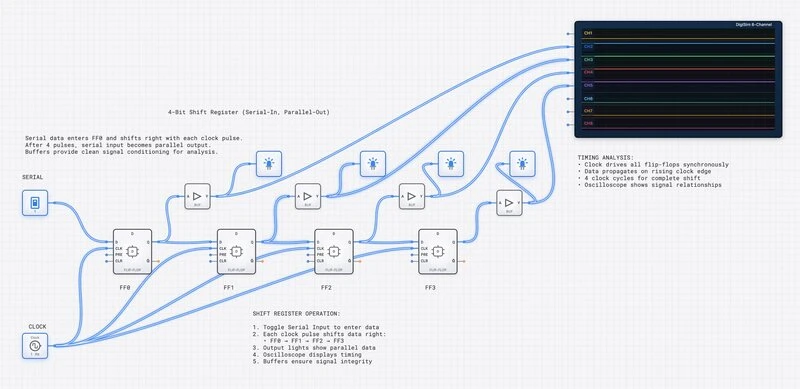
4-Bit SIPO Shift Register
Four rising-edge D flip-flops form a serial-in, parallel-out register with SI entering Q0 and stored bits advancing toward Q3. Buffered lights and four scope channels expose Q0..Q3; no clear, preset, parallel-load, direction, or serial-output path is connected.Open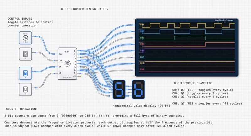
8-Bit Counter with Enable and Clear
The counter advances modulo 256 on rising edges when EN is HIGH and clears asynchronously when CLR is HIGH. Its connected LD switch is reserved by the current evaluator and does not load a value; two hexadecimal displays show 00 through FF.Open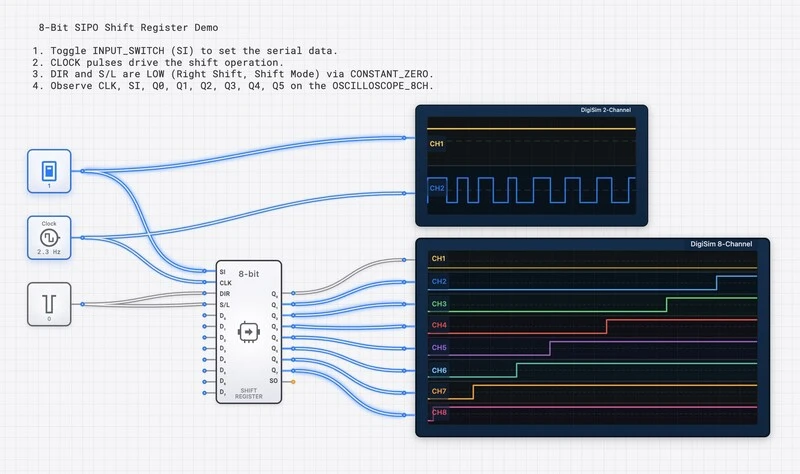
8-Bit SIPO Shift Register
An 8-bit register shifts SI toward Q0 on each rising clock edge with direction and mode fixed LOW. One scope shows SI and clock, while an 8-channel scope shows Q0..Q7; SO is not connected.Open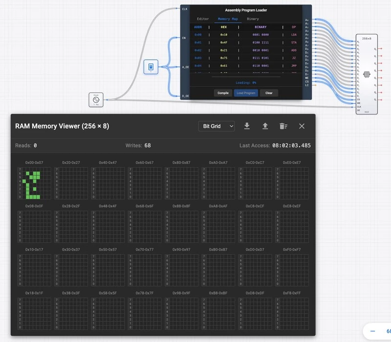
Assembly Loader and RAM Write Path
A clocked assembly program loader writes an eight-byte compiled image into 256 × 8 RAM through address, data, WE, and CS connections. RAM outputs are unconnected, so the circuit demonstrates loading rather than a visible read path.Open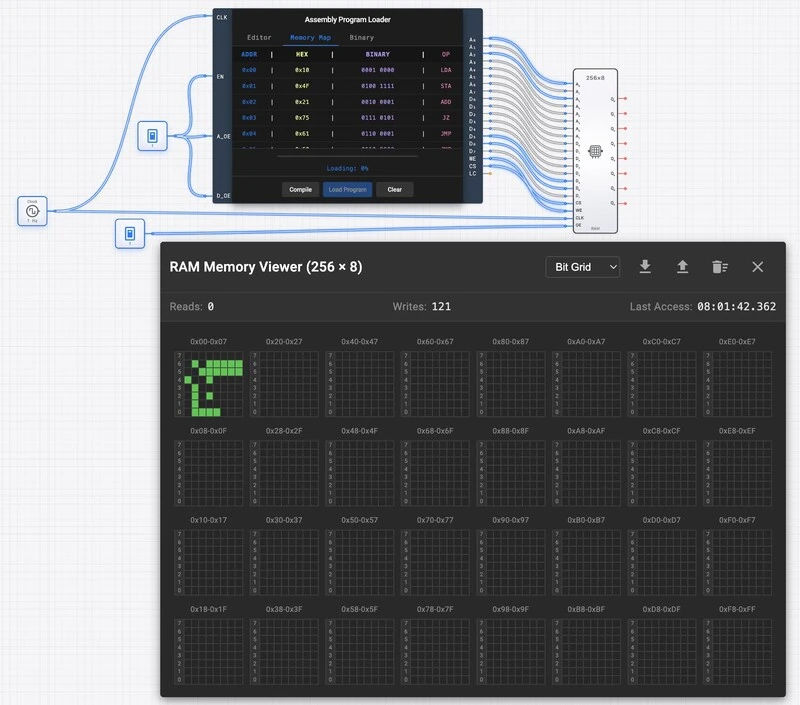
Assembly Program Loader to RAM
A clocked loader writes eight compiled bytes to addresses 0 through 7 of a 256 × 8 RAM. The second switch controls RAM OE, but the unconnected outputs provide no visible readback in this circuit.Open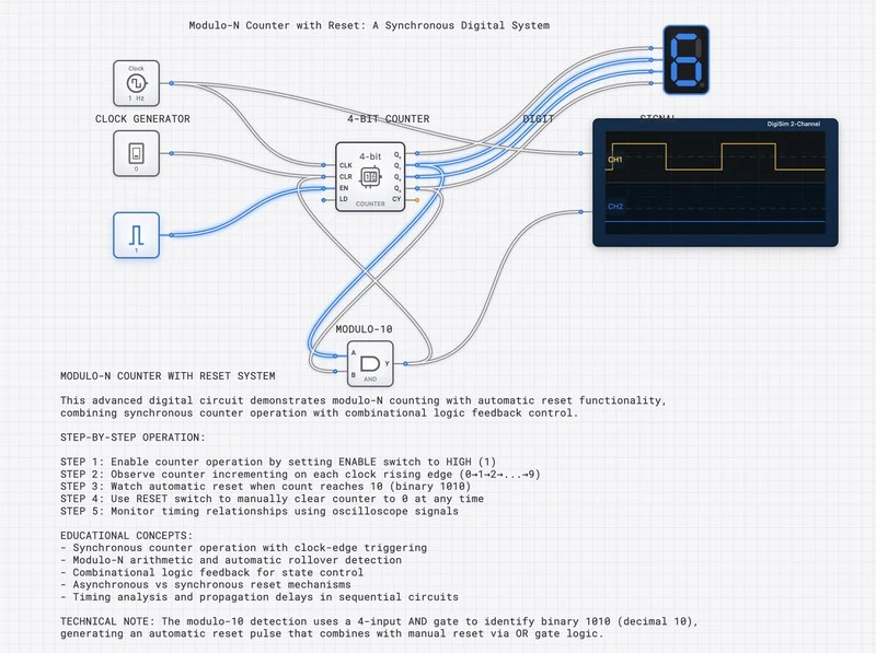
Modulo-10 Counter Reset-Wiring Diagnostic
A Q3 AND Q1 detector and a manual switch drive the counter's clear input directly, creating contention instead of the intended OR function. The saved circuit is a wiring diagnostic, not a functioning or programmable modulo-N counter.Open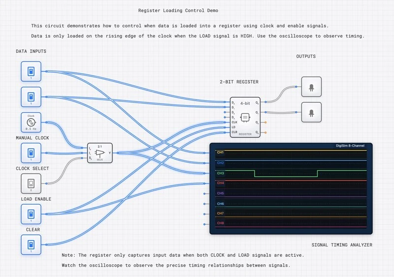
Register Load and Clock Selection
A 2-to-1 multiplexer selects an automatic or manual clock for a 4-bit register used here as a 2-bit demonstration. Load controls capture, clear acts asynchronously, and the scope shows D0, D1, selected clock, and load rather than Q.Open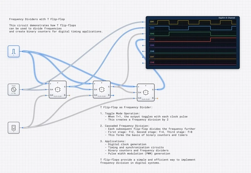
Three-Stage T Flip-Flop Frequency Divider
Three rising-edge T flip-flops form an asynchronous ripple divider with divide-by-2, divide-by-4, and divide-by-8 outputs. An active-HIGH asynchronous reset clears every stage, and the scope displays digital state traces rather than physical timing.Open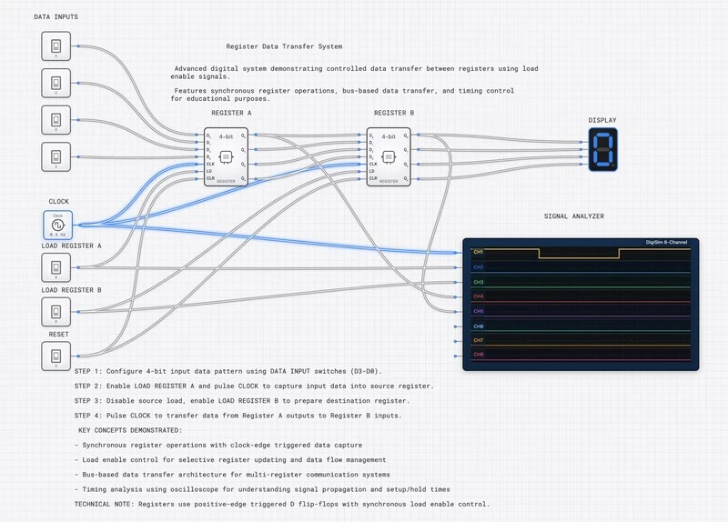
Unidirectional Register Transfer
Register A captures a 4-bit switch word, and Register B can capture A's outputs on a later shared clock edge. Independent load controls and a shared asynchronous reset are provided; there is no shared bus, arbitration, or reverse transfer.OpenCPU Components
7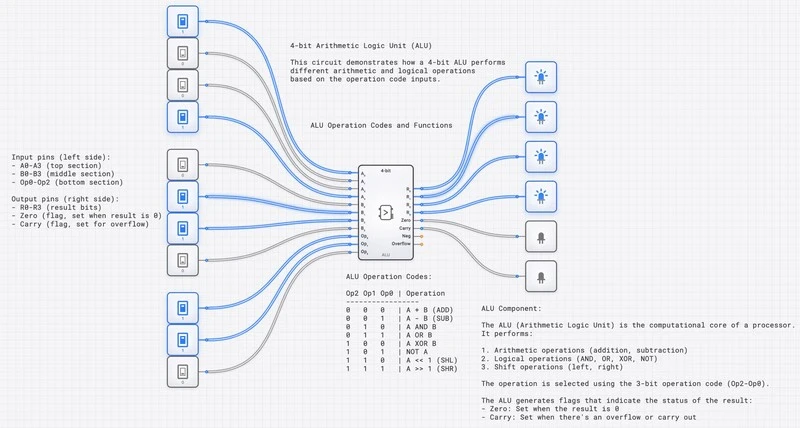
4-Bit ALU with Status Outputs
A packaged ALU applies one of eight arithmetic, Boolean, or shift operations to two 4-bit operands. Four result lights expose R3..R0, while two additional lights show Zero and the operation-dependent carry, borrow, or shifted-out bit.Open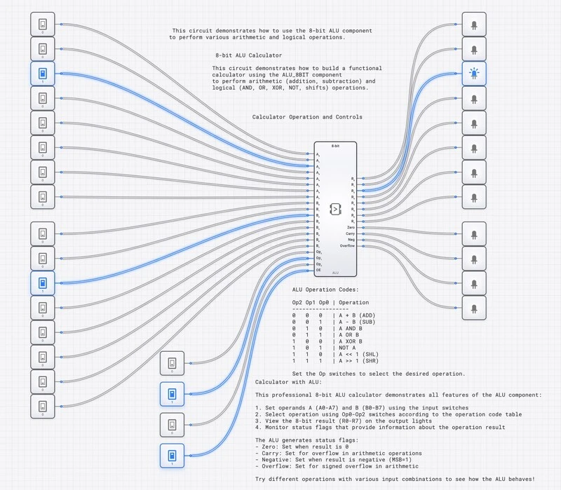
8-Bit ALU with Output Enable
A packaged 8-bit ALU provides eight arithmetic, Boolean, and shift operations plus Zero, Carry/Borrow, Negative, and Overflow outputs. OE releases all twelve outputs to high impedance when LOW.Open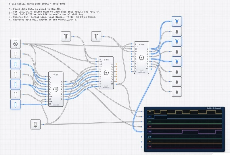
8-Bit Serial Shift Path
A PISO stage sends the fixed byte 0xAA LSB-first to a SIPO receiver on a shared clock. The circuit demonstrates parallel-load, serial-shift, and parallel-observe behavior but implements no UART or SPI framing, synchronization, or error detection.Open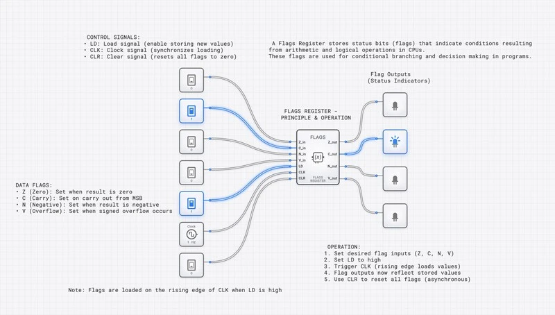
CPU Flags Register
A rising-edge flags register stores manually supplied Z, C, N, and V bits when load is enabled, with asynchronous clear. The circuit demonstrates flag storage only; it contains no ALU or logic that derives flags from an operation.Open
Intel 4004-Inspired 4-Bit CPU
A pedagogical 4-bit CPU follows FETCH, DECODE, EXECUTE, and STORE phases while a custom program computes 4 × 3 by repeated addition. It is inspired by the Intel 4004 but is not an emulator or binary-compatible implementation of the historical processor.Open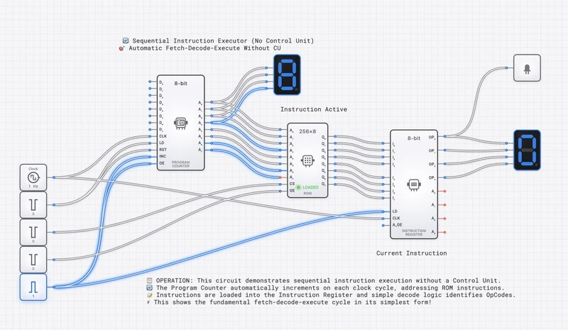
Program Counter–ROM–Instruction Register Fetch Path
An enabled program counter addresses ROM, and an instruction register captures the selected byte on the shared clock. The circuit has no decoder, control unit, ALU, branch path, or instruction-execution stage.Open