LOGIC LAB · TEMPLATES
回路テンプレート
デジタル論理設計のワークフローを加速するプロフェッショナルな回路テンプレート
注目のテンプレート
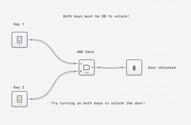
AND Gate Security System
Learn AND gate logic with a two-key security system. Both keys must be pressed to unlock the door. Perfect introduction to digital logic gates.
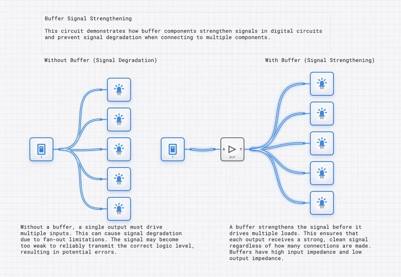
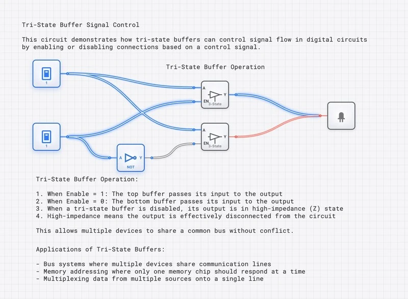
Buffer and Tri-State Demo
Buffer circuits demonstrating signal amplification and tri-state control. Learn about high-impedance states and bus systems.
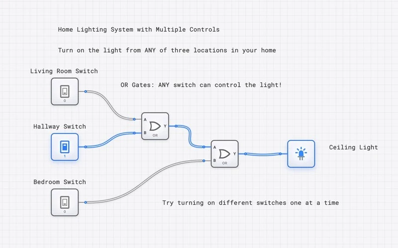
Multi-Switch OR Gate System
Multiple OR gates controlling a lighting system. Any switch can turn on the lights. Great for understanding parallel control systems.
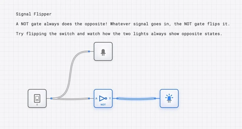
NOT Gate Signal Inverter
Simple NOT gate demonstration showing signal inversion. Input high makes output low and vice versa. Fundamental logic inversion concept.
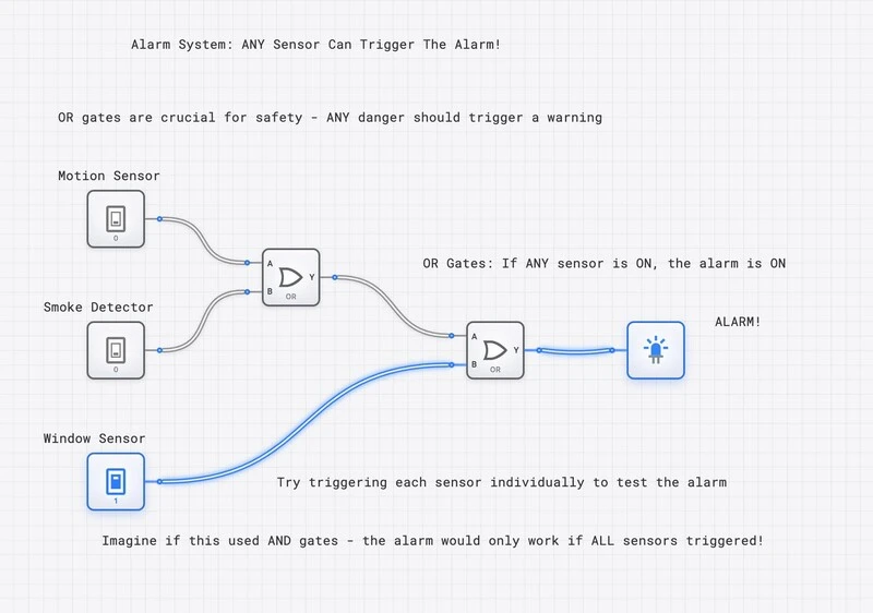
OR Gate Alarm System
Multi-sensor alarm using OR gates. Any sensor activation triggers the alarm. Learn how OR gates enable multiple trigger sources.
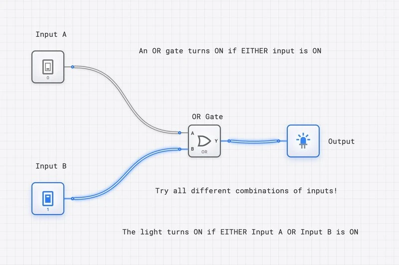
OR Gate Explorer
Interactive OR gate demonstration. Learn how OR gates work with visual feedback - any input can activate the output.
論理の基礎
AND Gate Security System
Learn AND gate logic with a two-key security system. Both keys must be pressed to unlock the door. Perfect introduction to digital logic gates.
Buffer and Tri-State Demo
Buffer circuits demonstrating signal amplification and tri-state control. Learn about high-impedance states and bus systems.
Multi-Switch OR Gate System
Multiple OR gates controlling a lighting system. Any switch can turn on the lights. Great for understanding parallel control systems.
NOT Gate Signal Inverter
Simple NOT gate demonstration showing signal inversion. Input high makes output low and vice versa. Fundamental logic inversion concept.
OR Gate Alarm System
Multi-sensor alarm using OR gates. Any sensor activation triggers the alarm. Learn how OR gates enable multiple trigger sources.
OR Gate Explorer
Interactive OR gate demonstration. Learn how OR gates work with visual feedback - any input can activate the output.
Single-Bit Tri-State Buffer
Basic tri-state buffer with enable control. Learn about high-impedance state and shared bus concepts in digital systems.
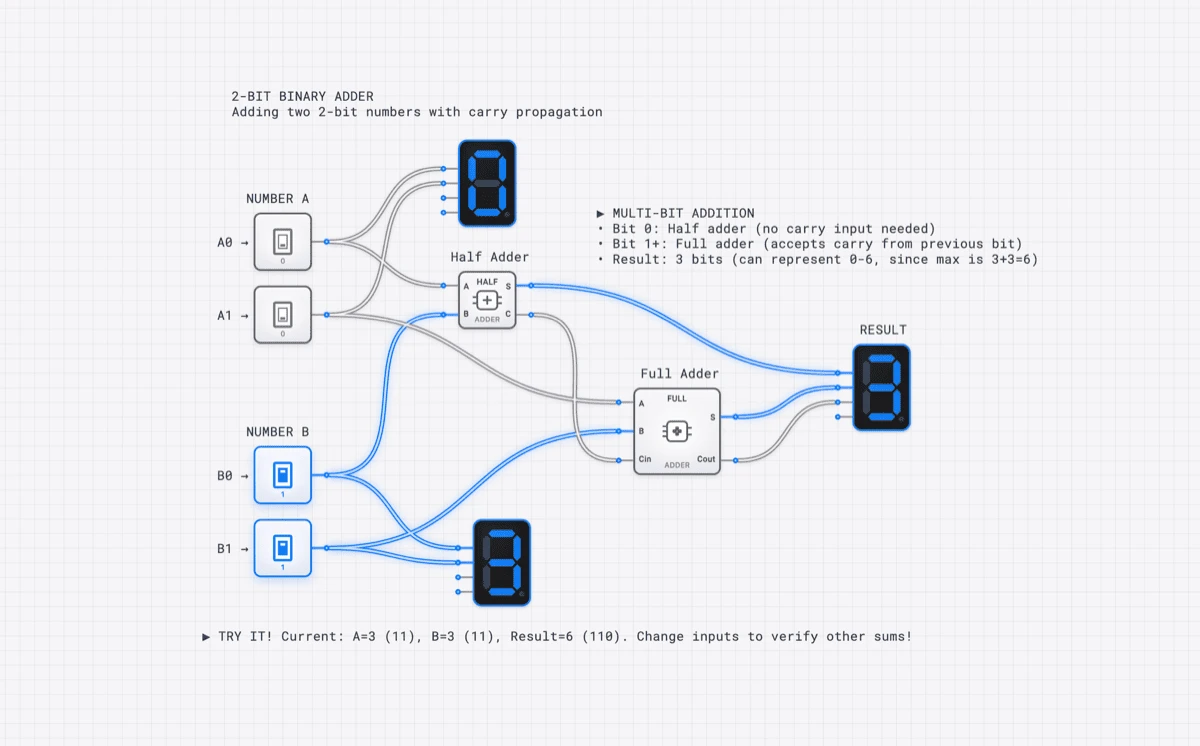
Template: 2-Bit Binary Adder
2 Bit Adder
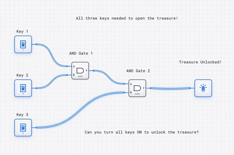
Triple AND Gate Treasure Chest
Explore cascaded AND gates with a three-key treasure chest. All three keys must be active to open the chest. Demonstrates multiple gate combinations.
派生ゲート
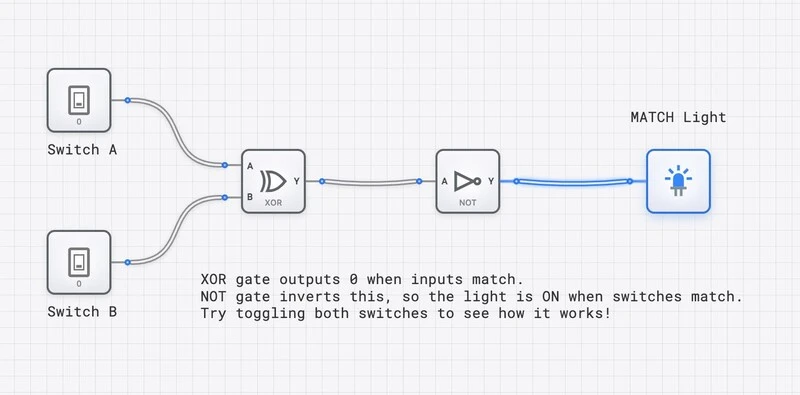
Simple Difference Detector
Basic XOR-based difference detector with NOT gate. Simple introduction to change detection using exclusive OR logic.
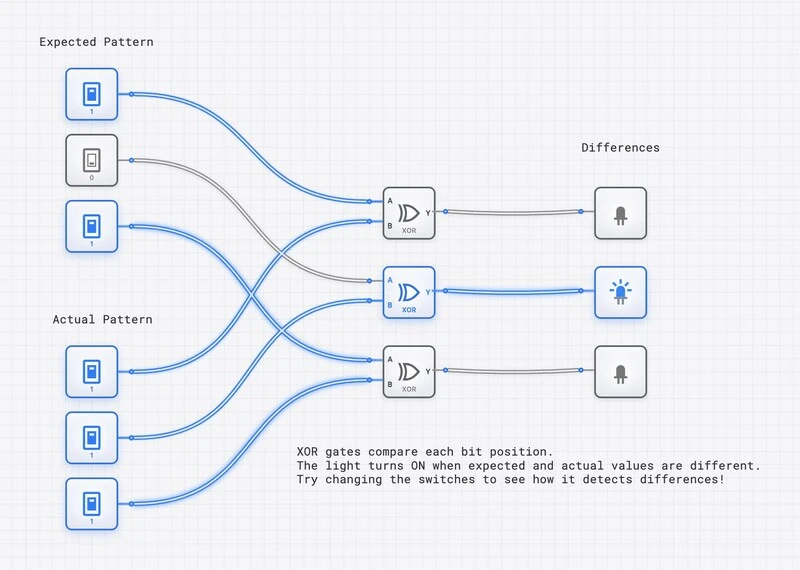
XOR Difference Detector
Multi-bit difference detection using XOR gates with oscilloscope visualization. Learn how XOR gates detect changes between inputs.
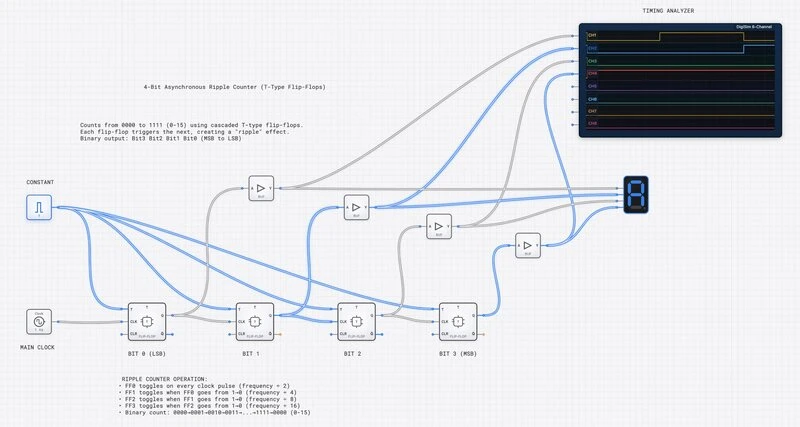
4-Bit Asynchronous Ripple Counter (T-Type Flip-Flops)
Counts from 0000 to 1111 (0-15) using cascaded T-type flip-flops. Each flip-flop triggers the next, creating a "ripple" effect. Binary output: Bit3 Bit2 Bit1 Bit0 (MSB to LSB)
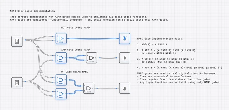
NAND Gate Universal Logic
NAND gate demonstration showing its universal property. Learn how NAND can implement other logic functions. Essential for understanding digital design.
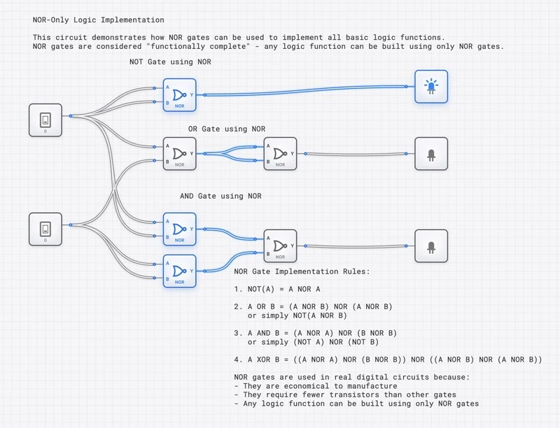
NOR Gate Universal Logic
NOR gate demonstration showing its universal property. Explore how NOR gates can create other logic functions. Complement to NAND universal logic.
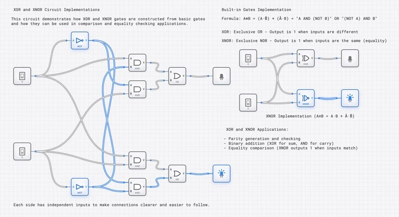
XOR and XNOR Gate Explorer
Comprehensive XOR and XNOR gate demonstration. Learn exclusive OR logic and its complement. Essential for understanding difference detection and parity.
組合せ論理
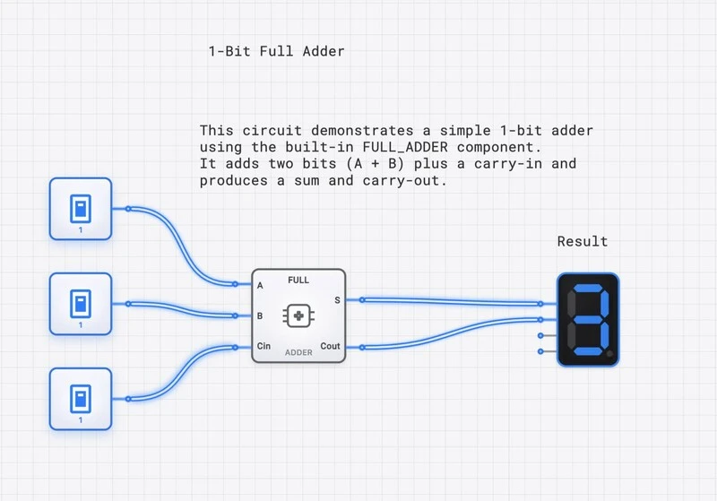
1-Bit Full Adder Component
Single full adder component with carry input and output. Foundation for multi-bit arithmetic circuits.
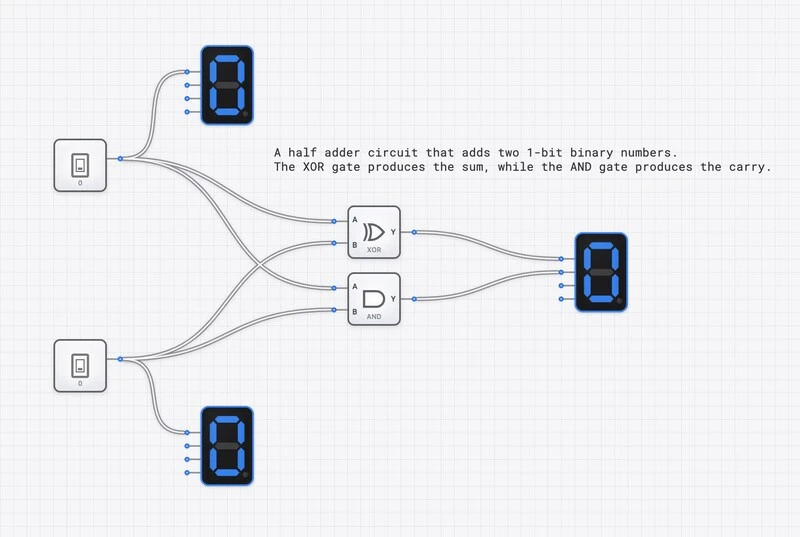
1-Bit Half Adder
Template: Template: 1-Bit Half Adder - Fundamental 1-bit addition using XOR and AND gates with digit display. Learn basic binary arithmetic and carry generation.
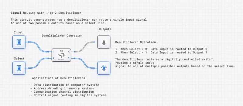
1-to-2 Demultiplexer
Basic demultiplexer routing one input to two outputs. Learn data distribution and addressing concepts.
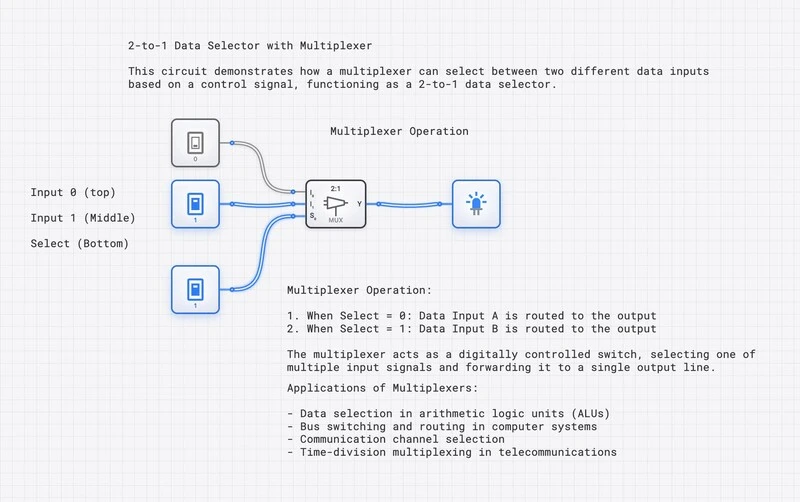
2-to-1 Multiplexer
Basic 2-input multiplexer with select control. Foundation for data selection and routing circuits.
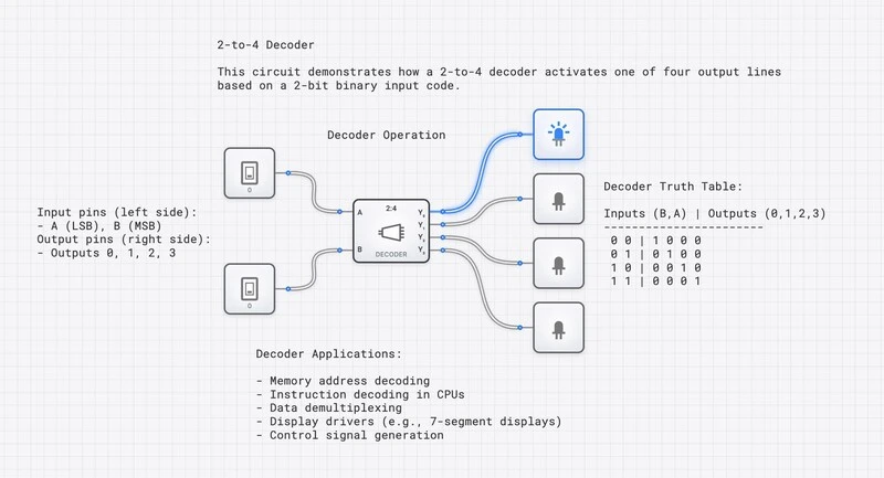
2-to-4 Decoder
Two-bit decoder creating four output lines. Learn address decoding for memory and device selection.
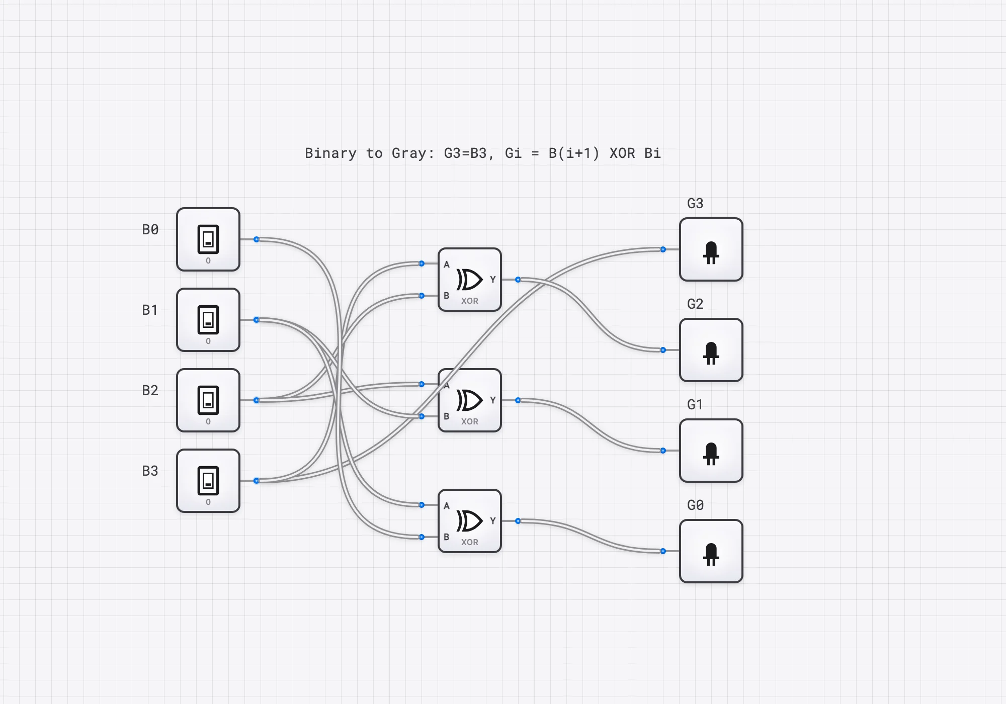
Binary to Gray Code Converter
Converts a 4-bit binary number to Gray code, where consecutive values differ by exactly one bit. Each Gray bit is an XOR of adjacent binary bits.
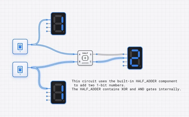
Half Adder Component Demo
Half adder component demonstration with digit displays. Introduction to packaged arithmetic components in digital design.
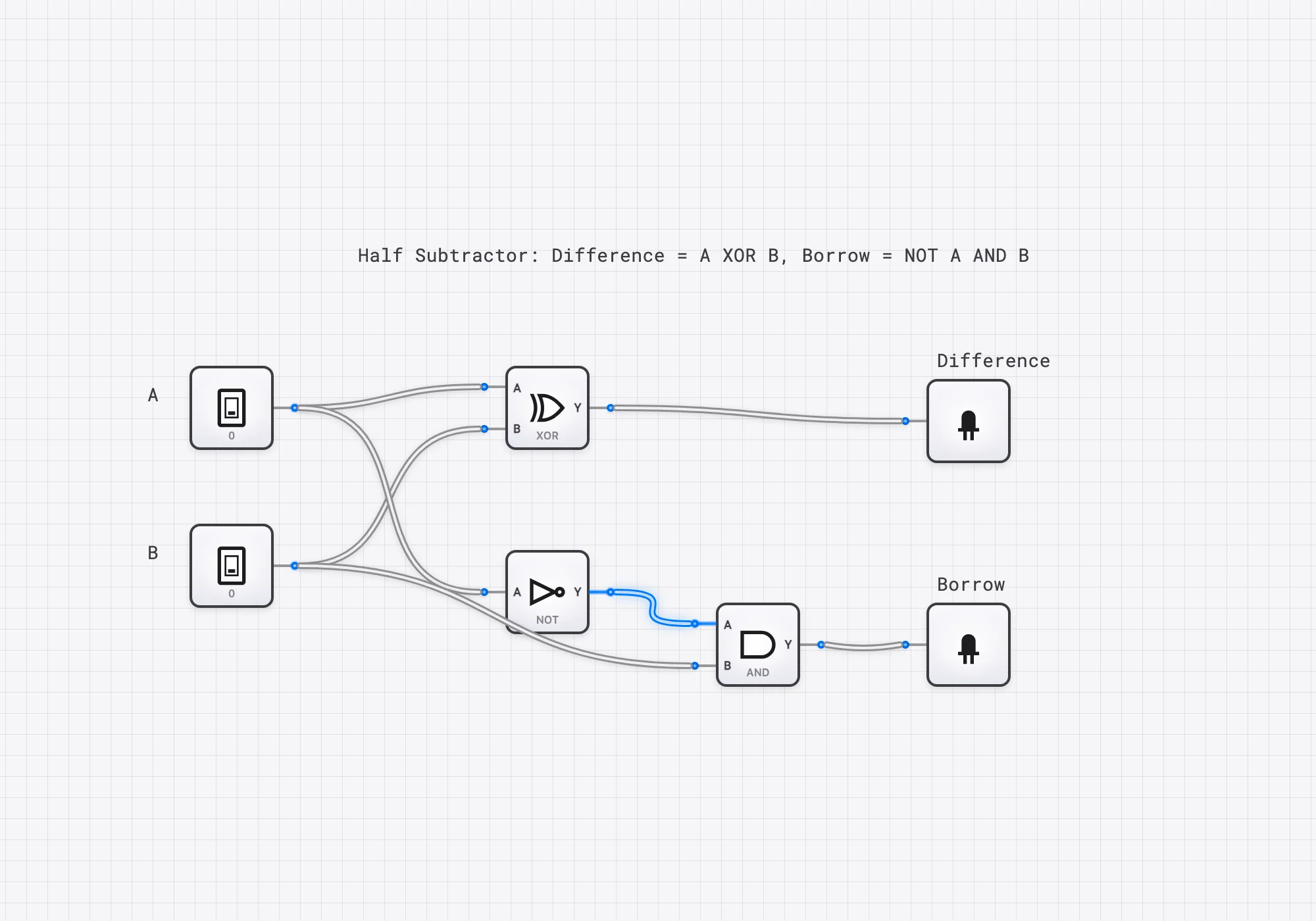
Half Subtractor
Subtracts one bit from another, producing a Difference bit and a Borrow bit. The complement of the half adder.
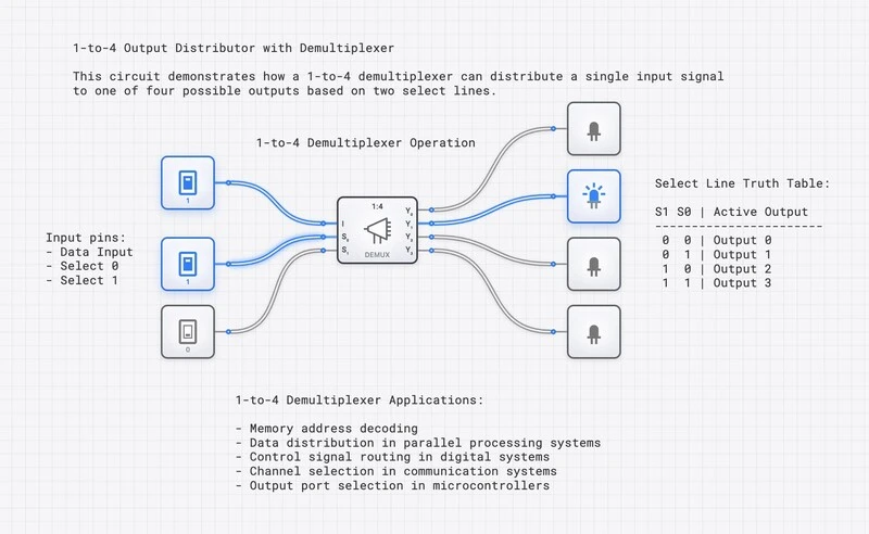
1-to-4 Demultiplexer
Four-output demultiplexer with address selection. Demonstrates address decoding and data distribution.
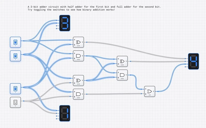
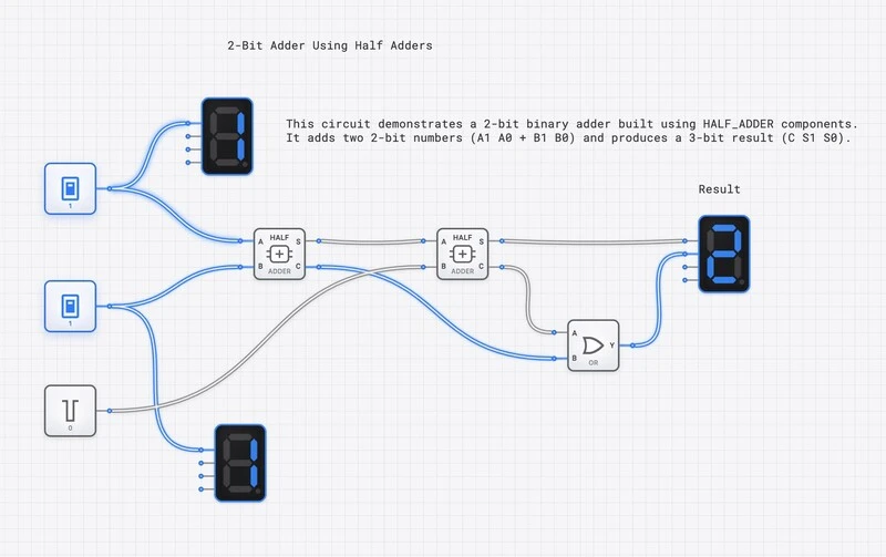
2-Bit Binary Adder
Two-bit binary addition with carry propagation. Demonstrates multi-bit arithmetic using basic gates and carry chain.
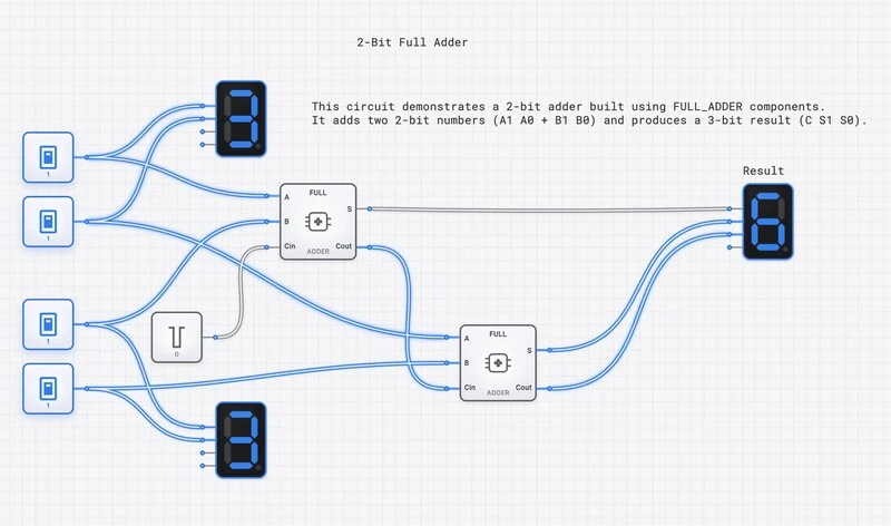
2-Bit Full Adder Chain
Two-bit full adder with carry propagation. Learn how full adders chain together for multi-bit arithmetic.
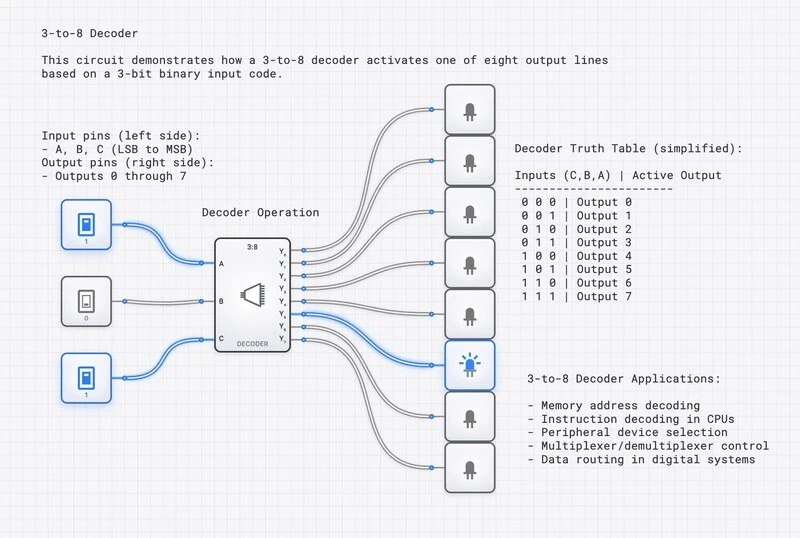
3-to-8 Decoder
Three-bit decoder with eight outputs. Advanced address decoding for larger memory and I/O systems.
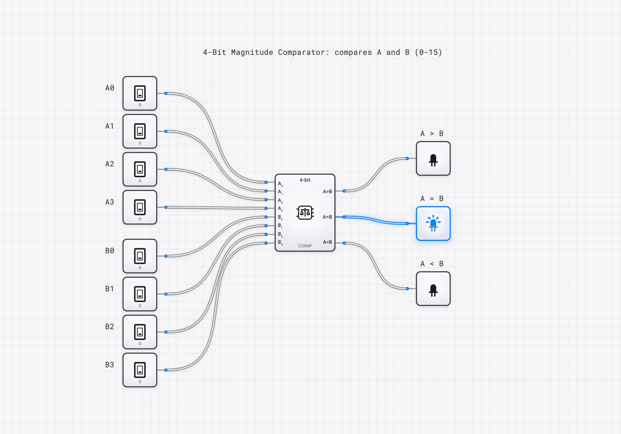
4-Bit Magnitude Comparator
Compares two 4-bit numbers A and B and asserts one of three outputs: A greater than B, A equals B, or A less than B.
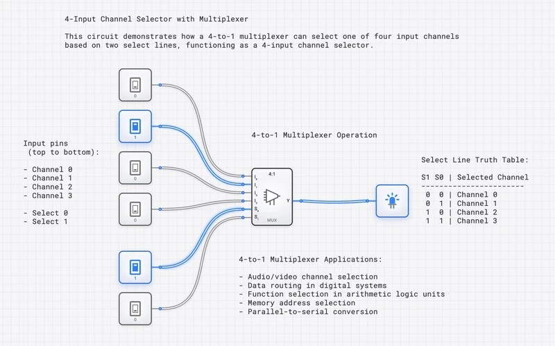
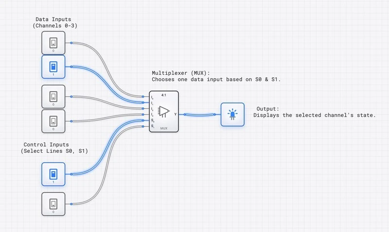
4-to-1 Multiplexer
Four-input multiplexer with 2-bit selection. Learn multi-input data routing and selection logic.
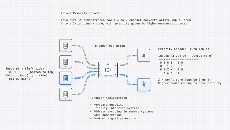
4-to-2 Priority Encoder
Four-input priority encoder creating 2-bit output. Learn data compression and priority encoding schemes.
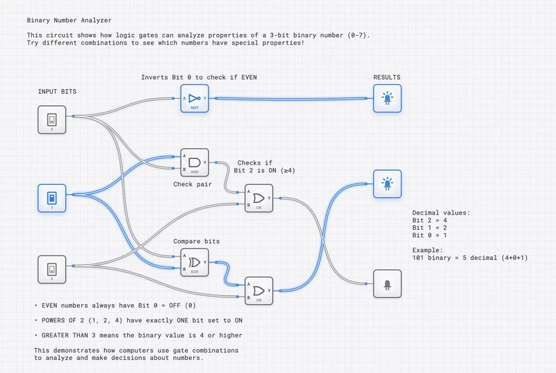
Binary Number Analyzer
Multi-gate circuit analyzing 3-bit binary numbers. Uses NOT, AND, OR, and XOR gates to detect patterns and properties in binary data.
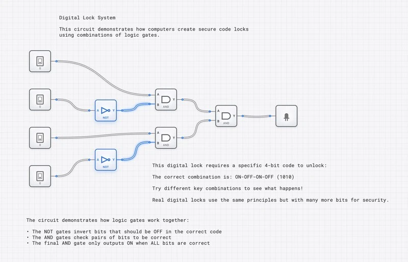
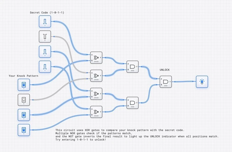
Digital Lock Security System
Advanced security system using NOT and AND gates. Specific combination required to unlock. Demonstrates complex boolean logic implementation.
Full Adder with Carry
Full adder circuit using half adders and OR gate. Learn carry input handling and full arithmetic operations.
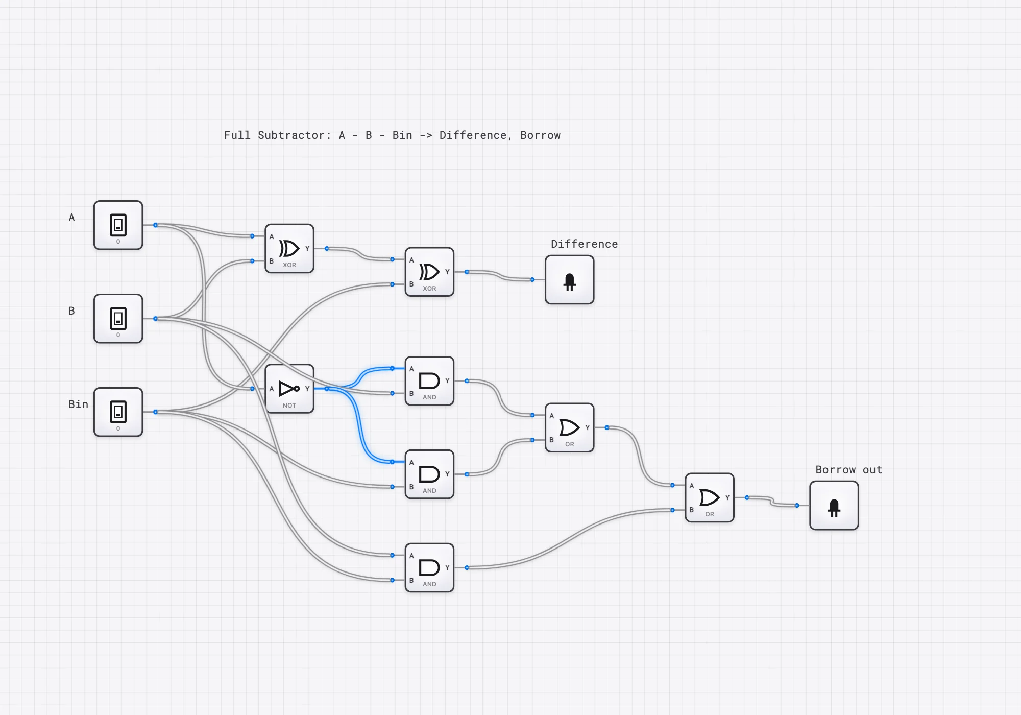
Full Subtractor
Subtracts two bits and an incoming borrow, producing a Difference and an outgoing Borrow. Chains to build multi-bit subtractors.
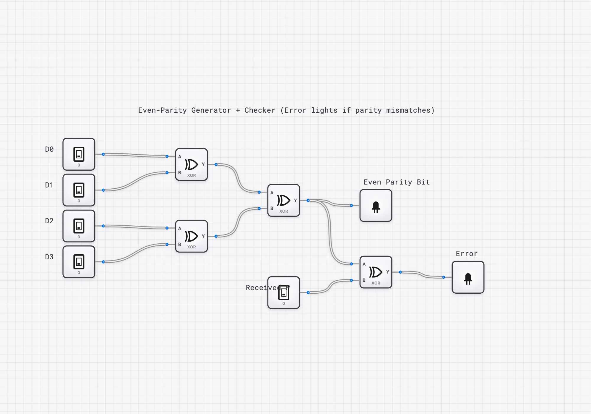
Parity Generator and Checker
Generates an even-parity bit for 4 data bits with an XOR tree, then checks a received parity bit for single-bit transmission errors.
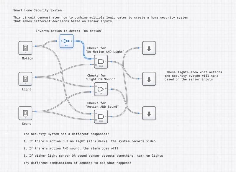
Smart Robot Decision Logic
Complex decision-making circuit using multiple gate types. Robot logic with sensors, NOT gates, AND gates, and OR gates for intelligent behavior.
TV Channel Selector MUX
4-to-1 multiplexer selecting TV channels. Learn data routing and selection using multiplexer logic for real-world applications.
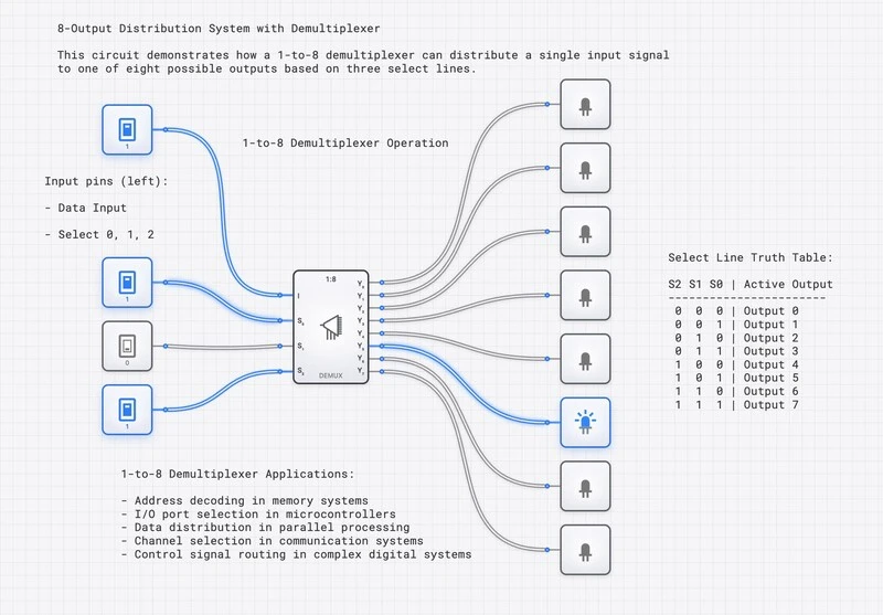
1-to-8 Demultiplexer
Eight-output demultiplexer with 3-bit address selection. Advanced data routing for complex systems.
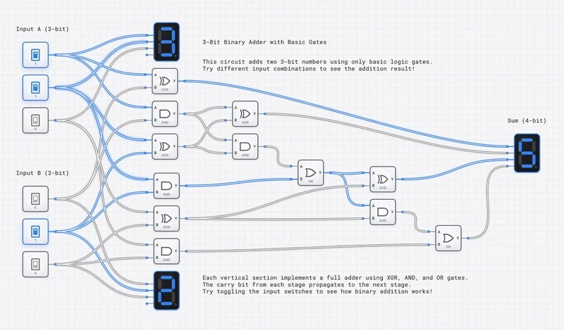
3-Bit Binary Adder
Complex 3-bit adder with full carry propagation. Advanced arithmetic circuit demonstrating cascaded carry logic.
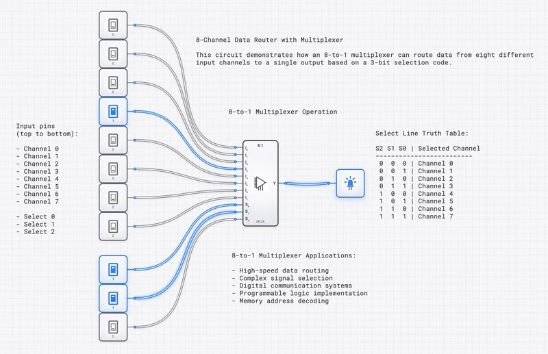
8-to-1 Multiplexer
Eight-input multiplexer with 3-bit selection. Complex data routing for advanced digital systems.
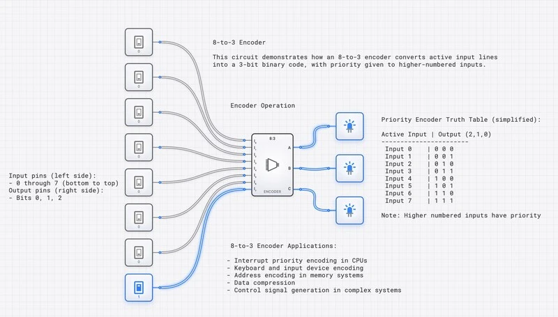
8-to-3 Priority Encoder
Eight-input priority encoder with 3-bit output. Advanced data compression and interrupt handling concepts.
Complex Logic Circuit Demo
Advanced multi-gate circuit using XNOR, AND, and various constants. Complex boolean logic implementation for advanced learners.
出力と表示
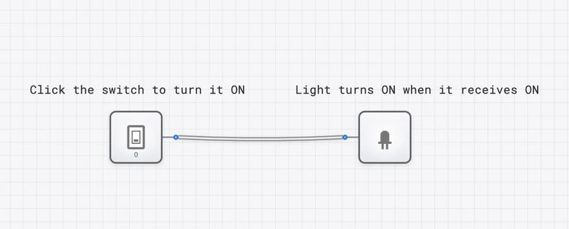
Basic Switch and Light Demo
Simple switch-to-light connections demonstrating basic digital input and output. Perfect starting point for digital circuit exploration.
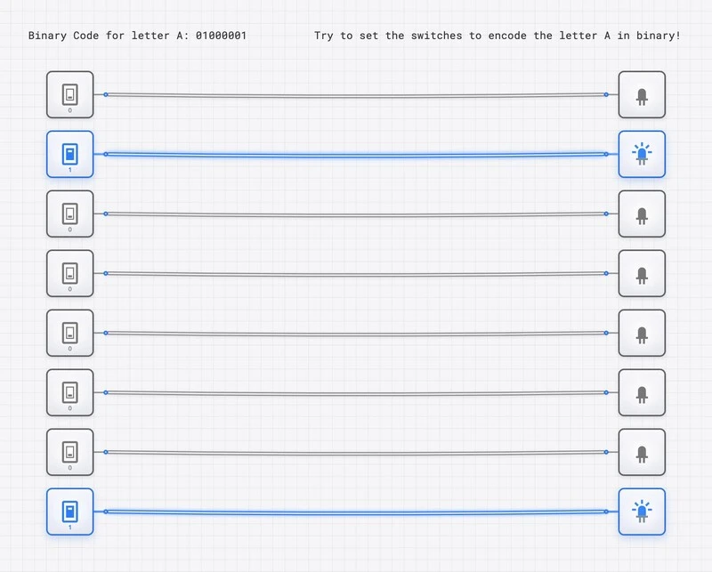
Multi-Switch Control Panel
Multiple independent switch-light pairs. Learn basic digital I/O concepts with visual feedback. Foundation for more complex circuits.
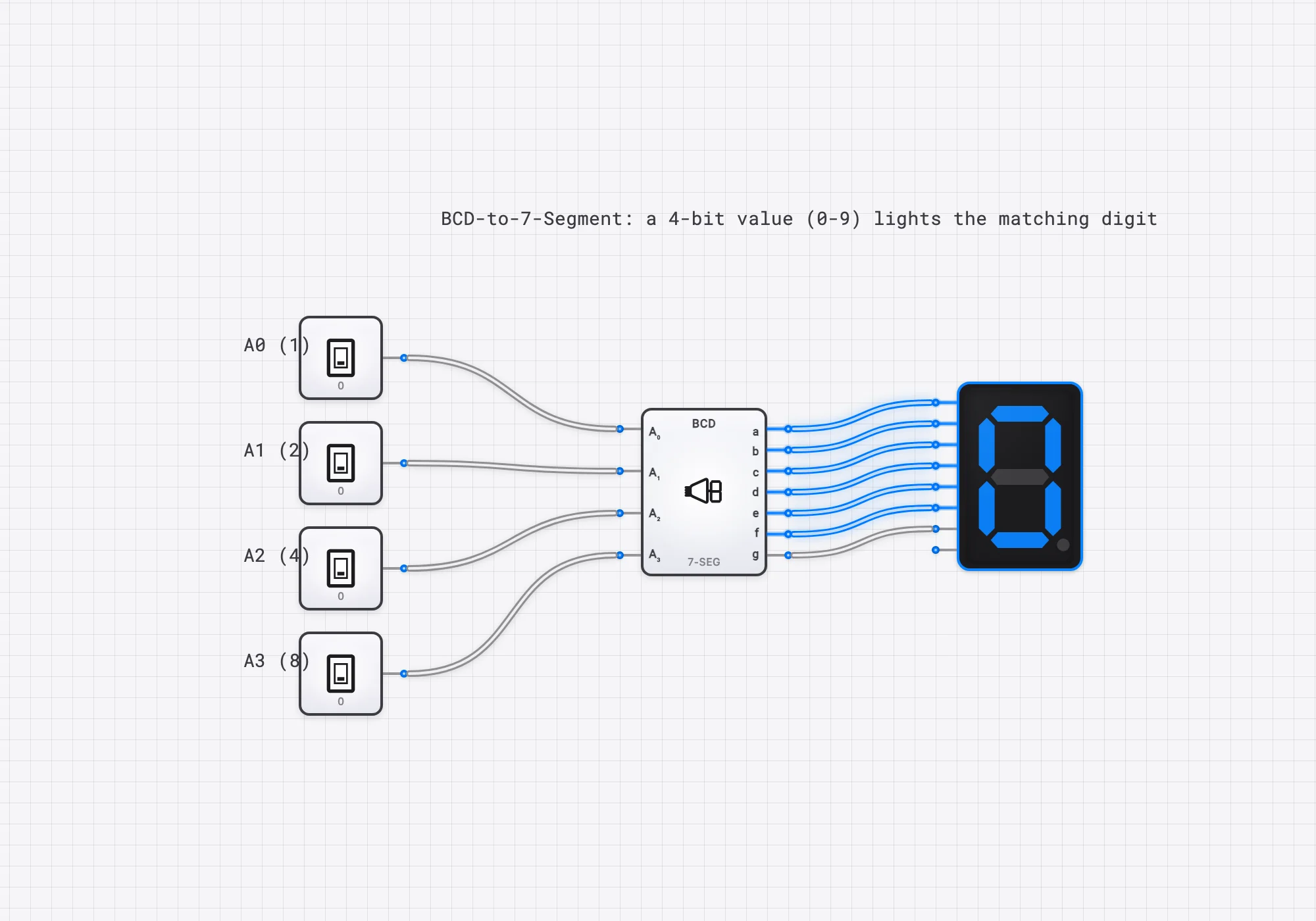
BCD to 7-Segment Display
Turns a 4-bit BCD value into a decimal digit on a seven-segment display using a BCD-to-7-segment decoder. The bridge between counting logic and a readable display.
順序論理
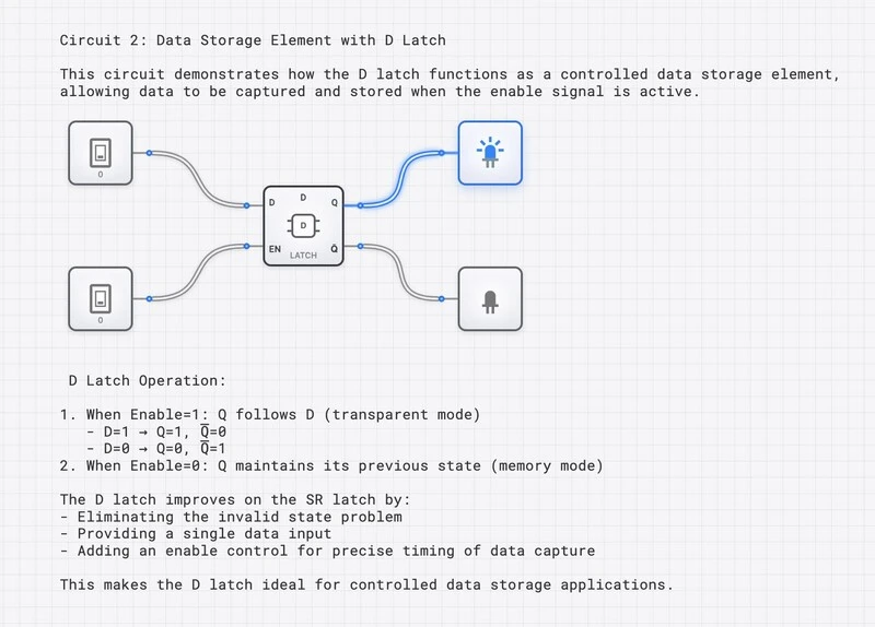
Basic D Latch
Simple D latch with data and enable inputs. Introduction to digital memory storage and transparent latch operation.
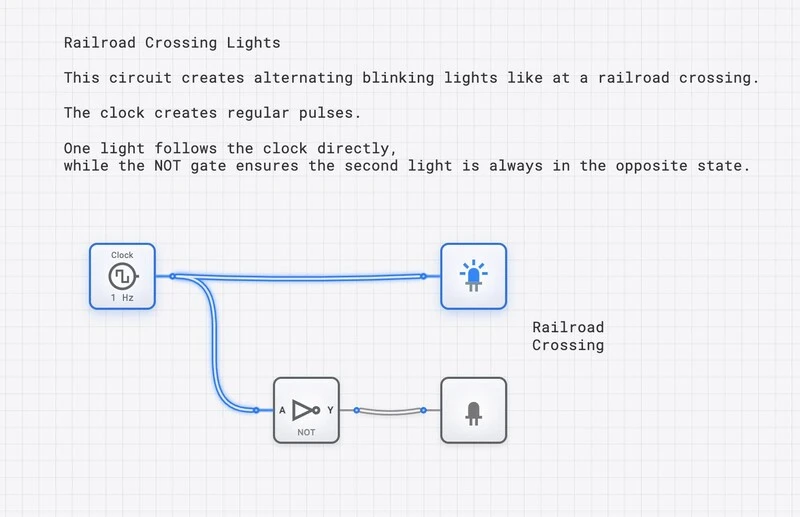
Clock-Driven Crossing Lights
Railroad crossing lights using clock and NOT gate. Learn about timing circuits and alternating outputs. Introduction to sequential timing.
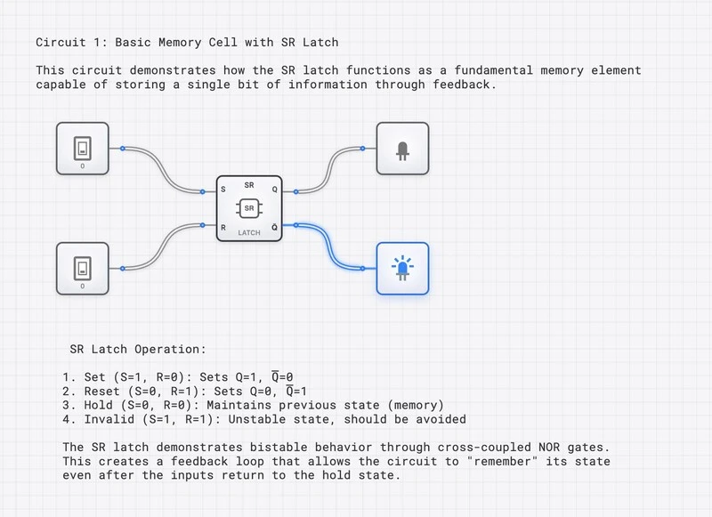
SR Latch Demonstration
Set-Reset latch with S and R inputs. Learn basic memory storage using cross-coupled gates and bistable operation.
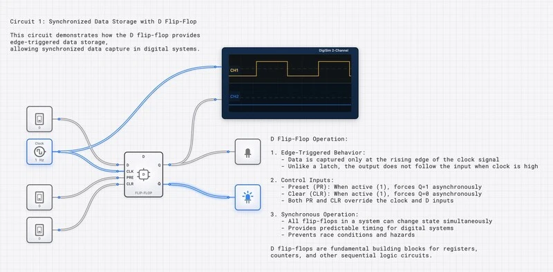
D Flip-Flop Edge Triggered
D flip-flop demonstrating edge-triggered operation. Learn difference between edge and level triggered storage.
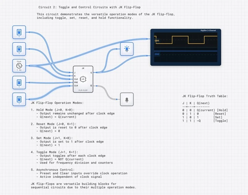
D Latch with Oscilloscope
D latch timing analysis with oscilloscope visualization. Study setup time, hold time, and propagation delay.
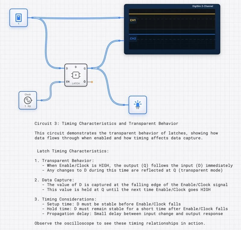
JK Flip-Flop Master-Slave
JK flip-flop with all input combinations and oscilloscope. Advanced flip-flop operation without race conditions.
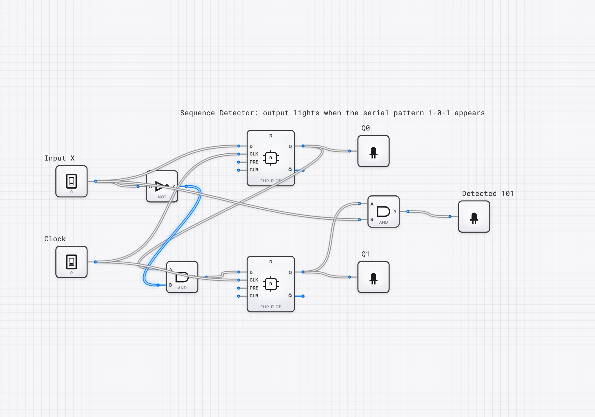
Sequence Detector (101)
A finite-state machine that watches a serial input and lights its output the instant the overlapping pattern 1-0-1 appears. Two D flip-flops hold the state, a little logic computes the next state and the Mealy output.
メモリシステム
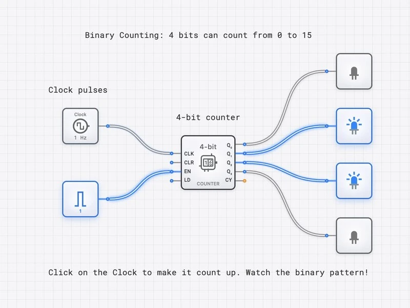
4-Bit Binary Counter
Template: Template: 4-Bit Binary Counter - Interactive 4-bit binary counter with visual output lights. Learn binary counting sequences and clock-driven operation. Count from 0 to 15 in binary.
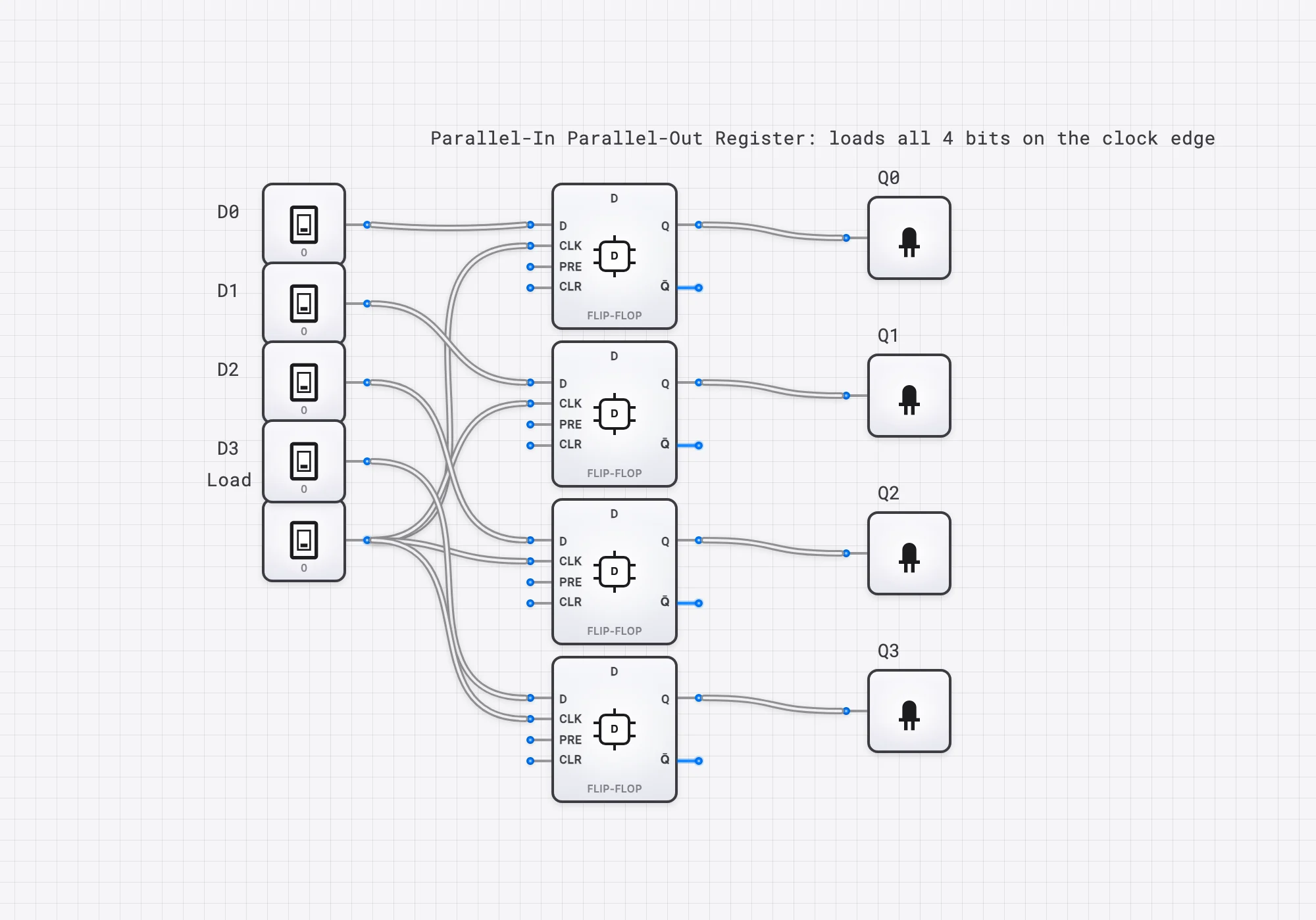
4-Bit PIPO Register
A parallel-in parallel-out register: four D flip-flops sharing a clock capture four input bits simultaneously and hold them.
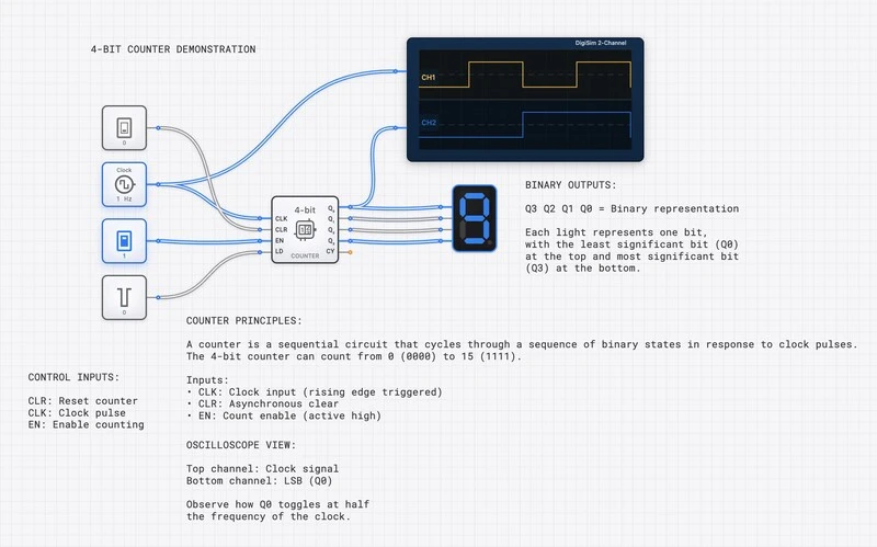
4-Bit Counter with Display
4-bit counter with digital display and oscilloscope timing. Learn counter operation and numerical display systems.
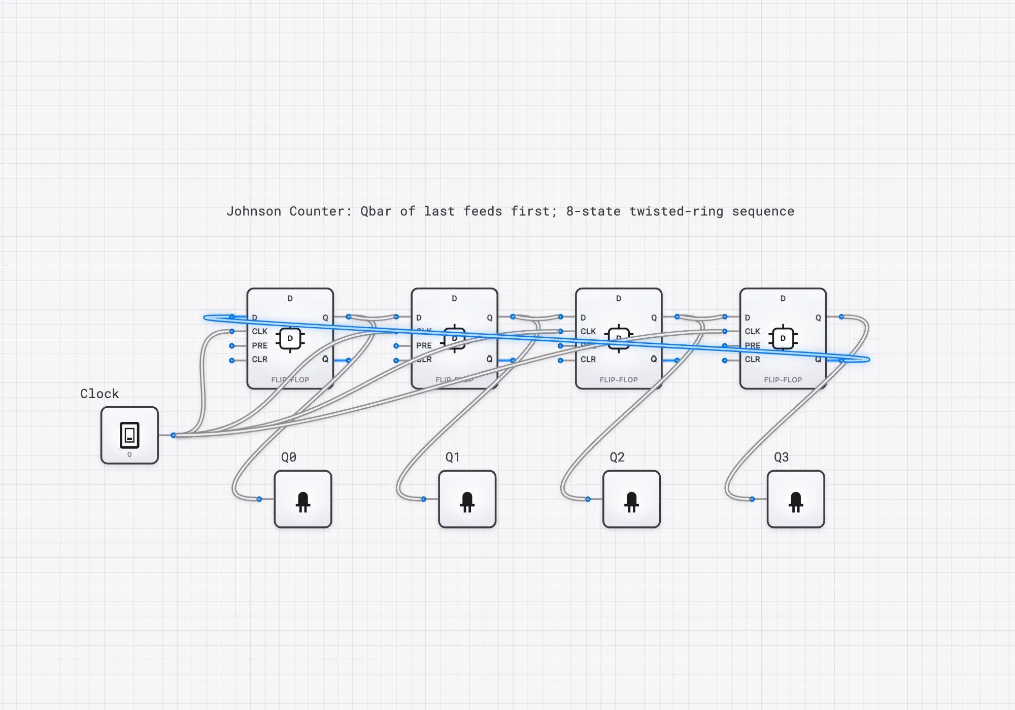
4-Bit Johnson Counter
A twisted-ring counter: the inverted output of the last flip-flop feeds the first, producing eight unique states from four flip-flops.
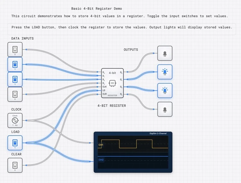
4-Bit Register with Clock
Basic 4-bit register with parallel load and clock. Foundation for data storage in digital systems with timing analysis.
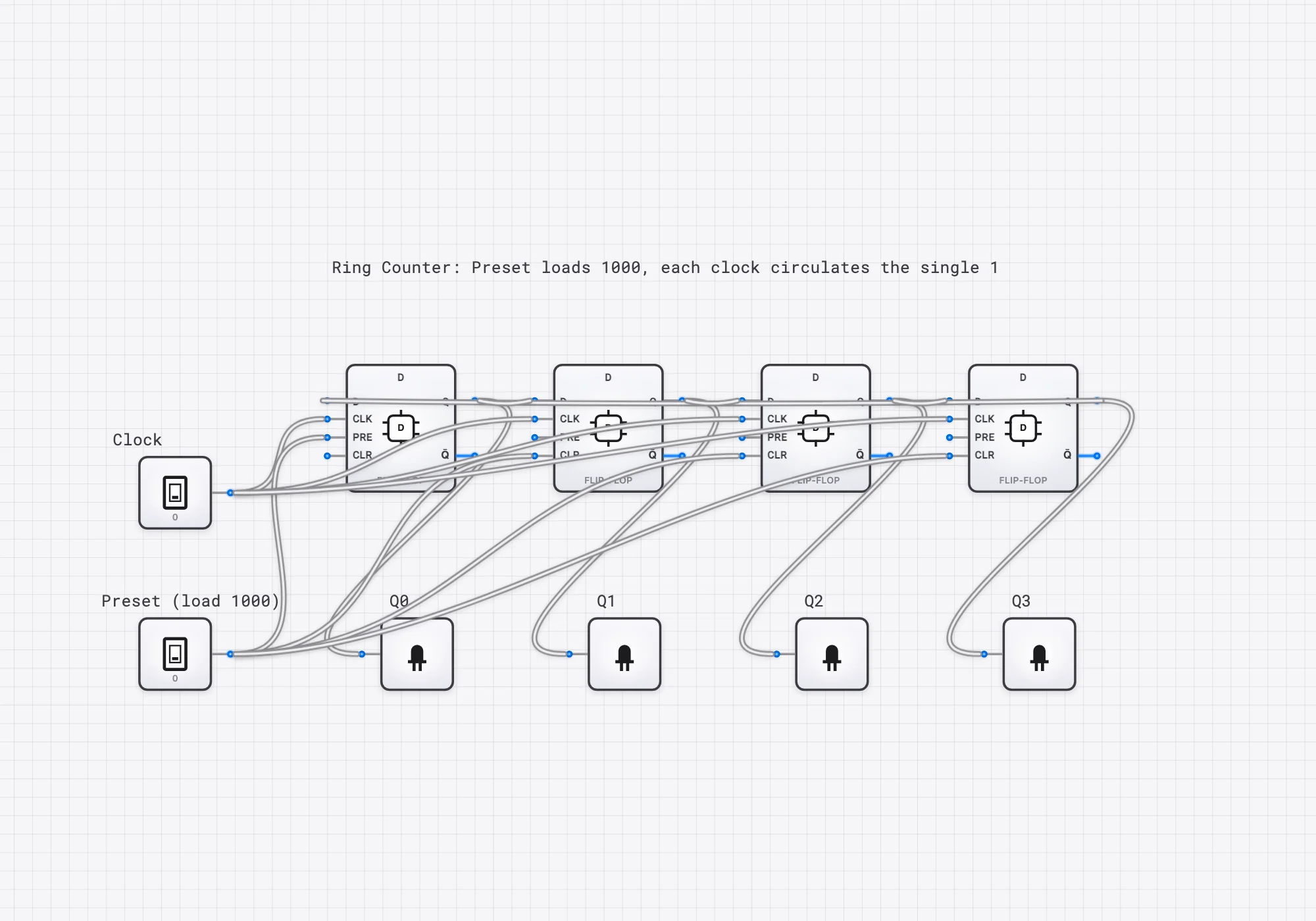
4-Bit Ring Counter
Four D flip-flops in a loop. The Preset input loads a single 1 (state 1000); each clock pulse then shifts that 1 around the ring, giving a one-hot sequence.
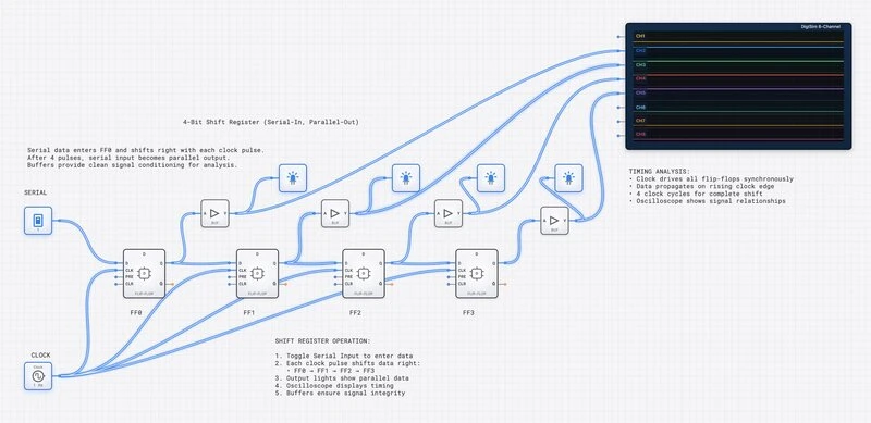
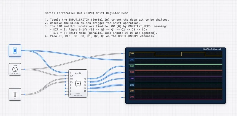
4-Bit Shift Register
This circuit is a 4-bit Serial-In, Parallel-Out (SIPO) Shift Register. Its primary function is to take a stream of data one bit at a time (serially) and store it. Once the data is stored in the register, all four bits can be read simultaneously (in parallel). It essentially converts data from a serial format to a parallel format
4-Bit Shift Register SISO
Serial-in, serial-out shift register with oscilloscope. Learn data shifting and serial communication concepts.
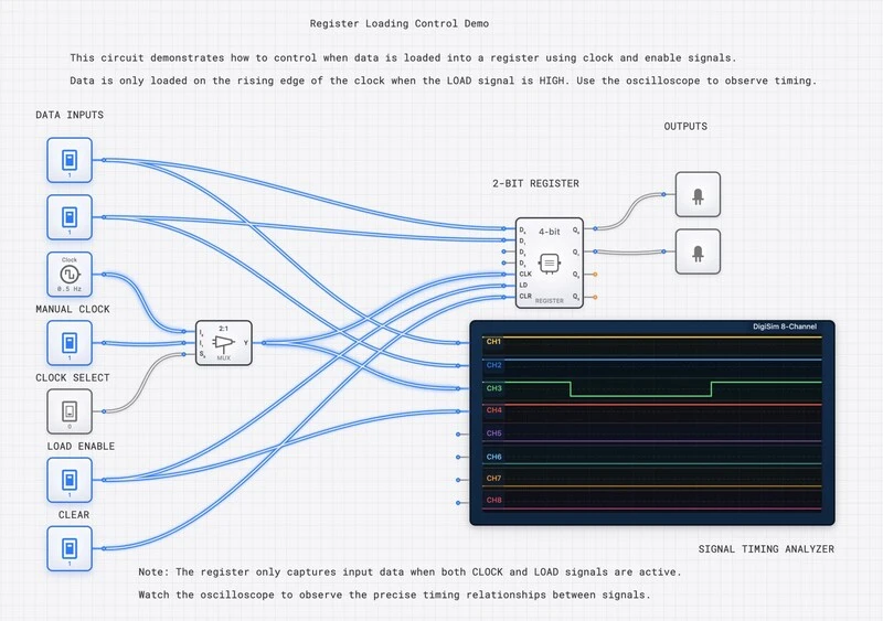
Register Load Control Demo
Register with load control and multiplexed input selection. Learn conditional data loading and register control signals.
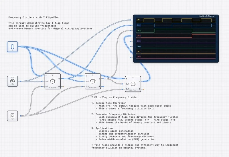
T Flip-Flop Frequency Divider
Toggle flip-flop chain creating frequency division. Learn how T flip-flops divide clock frequencies for timing circuits.
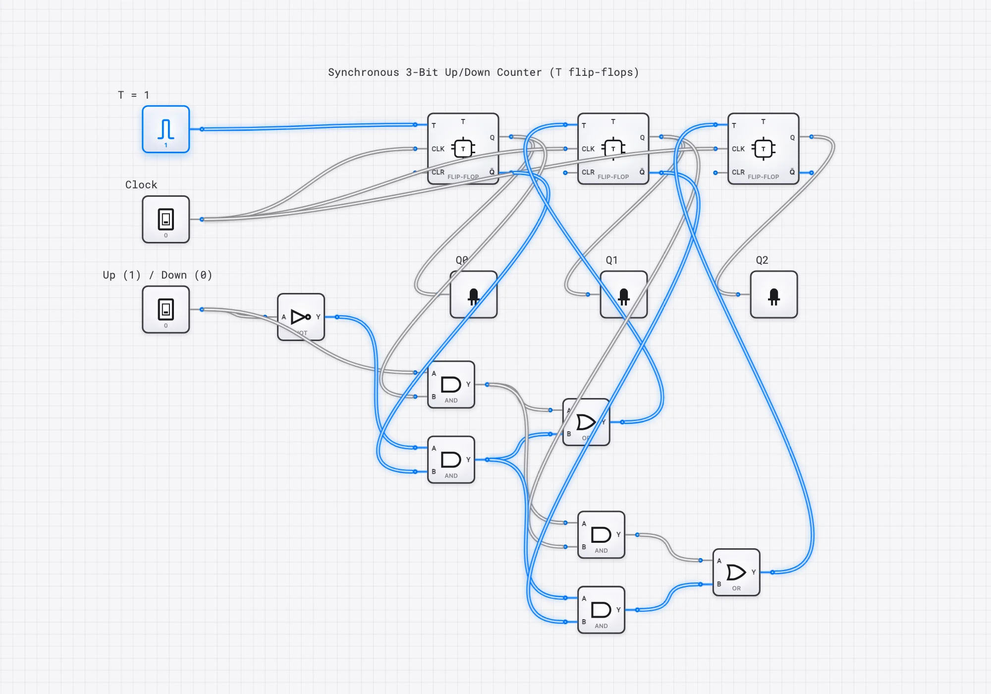
3-Bit Up/Down Counter
A synchronous 3-bit counter that counts up or down depending on a direction input. T flip-flops toggle under combinational steering logic so all bits change on the same clock edge.
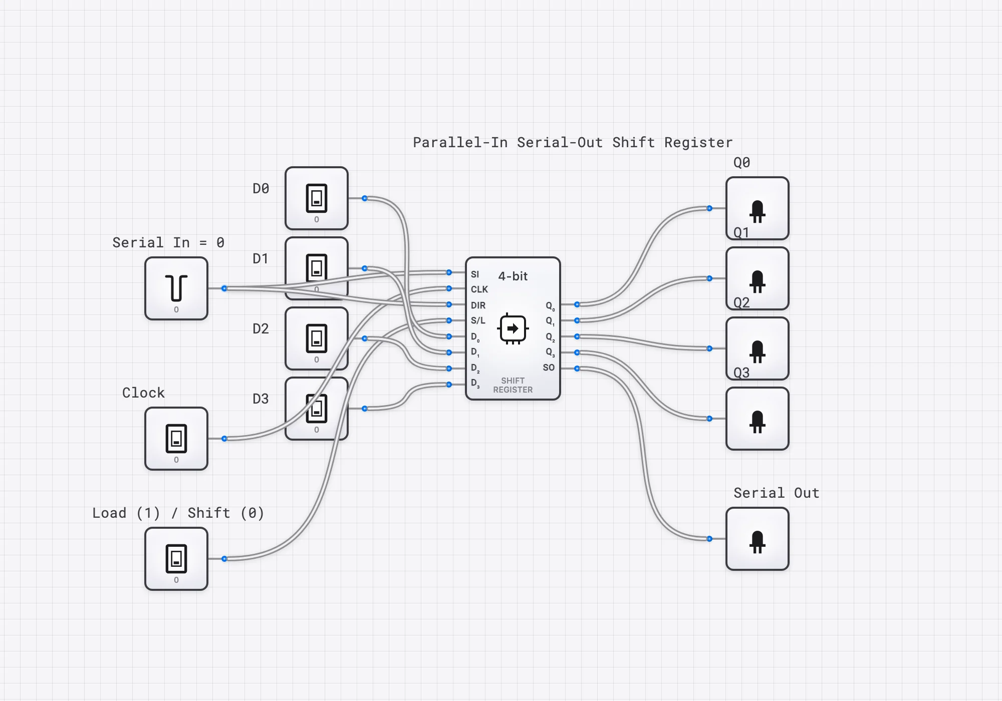
4-Bit PISO Shift Register
Loads four bits in parallel (Load = 1) then shifts them out one bit per clock on a single serial line (Load = 0). The parallel-in serial-out converter at the heart of serial transmitters.
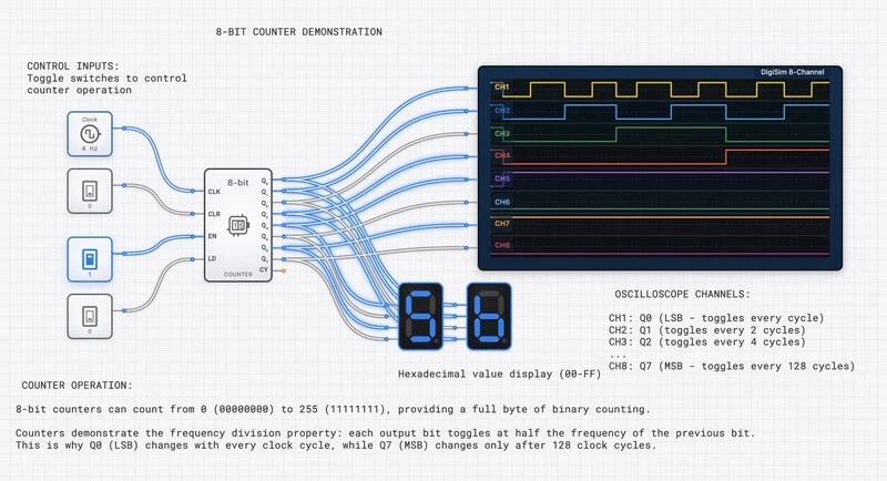
8-Bit Counter with Controls
8-bit counter with load, enable, and clear controls. Advanced counter operations with dual display outputs.
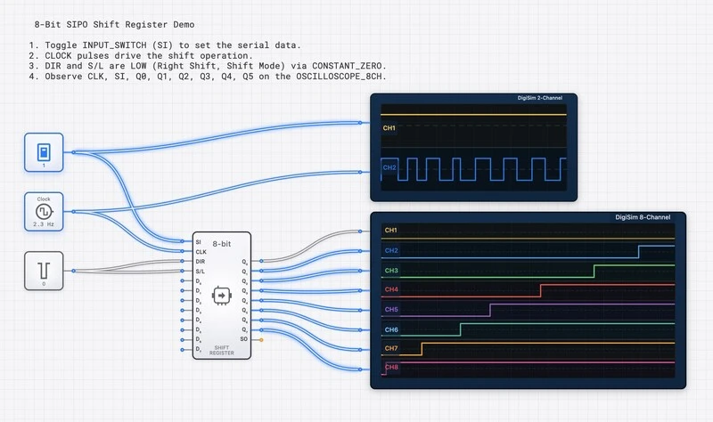
8-Bit SIPO Shift Register
8-bit serial-in, parallel-out shift register with dual oscilloscope. Advanced serial-to-parallel data conversion.
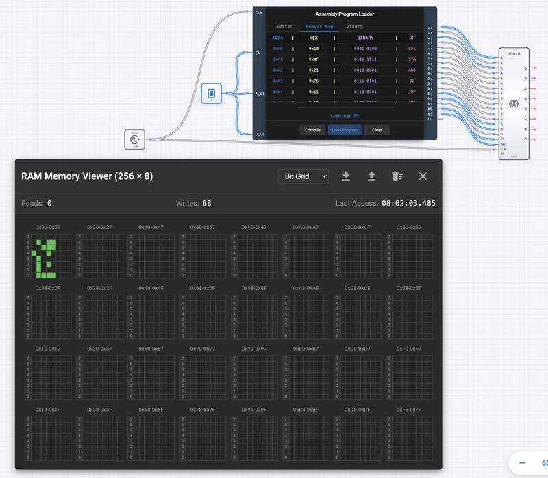
Basic RAM Memory System
RAM memory with program loader and clock control. Introduction to random access memory operation and addressing.
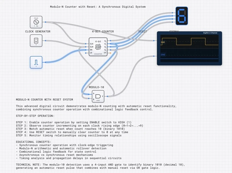
Modulo-N Counter with Reset
Programmable modulo-N counter with reset logic. Learn custom counting sequences and counter design techniques.
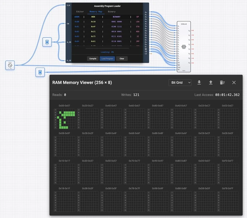
RAM with Address Control
Enhanced RAM system with address and data control switches. Advanced memory operations and data storage concepts.
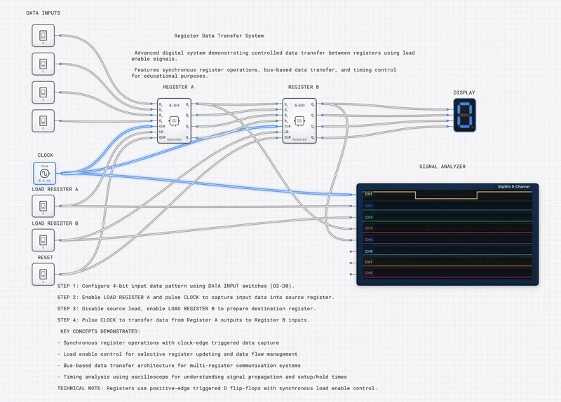
Register Data Transfer System
Complex register-to-register data transfer with multiplexers. Learn data bus operations and register file management.
CPUコンポーネント
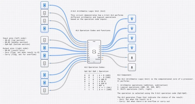
4-Bit ALU Demonstration
Complete 4-bit ALU performing arithmetic and logic operations. Advanced combinational circuit for CPU design.
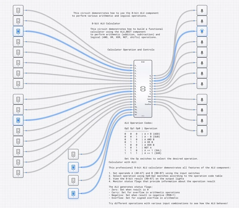
8-Bit ALU System
Professional 8-bit ALU with multiple operation modes. Complex arithmetic and logic unit for advanced processor design.
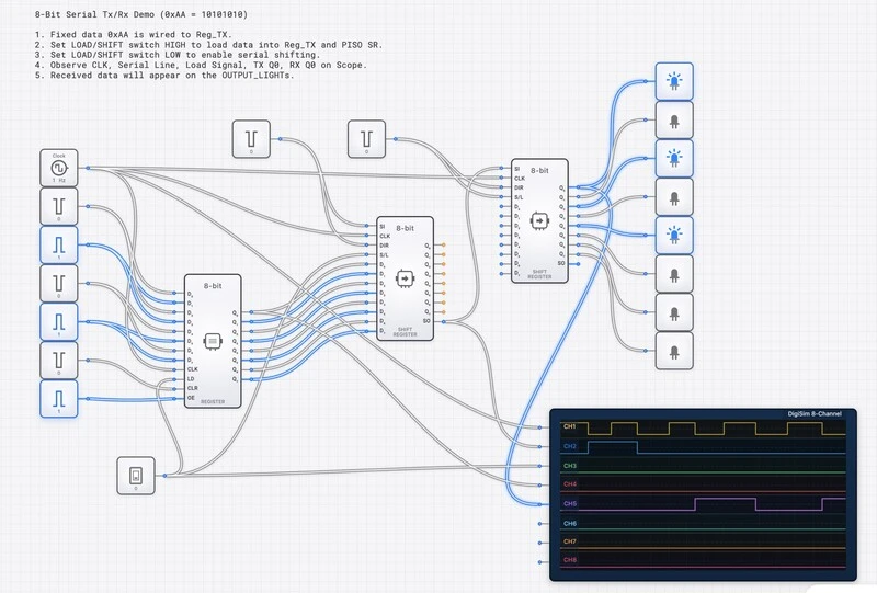
8-Bit Serial Transmitter Receiver
Complete serial communication system with transmit and receive shift registers. Learn UART-style data transmission.
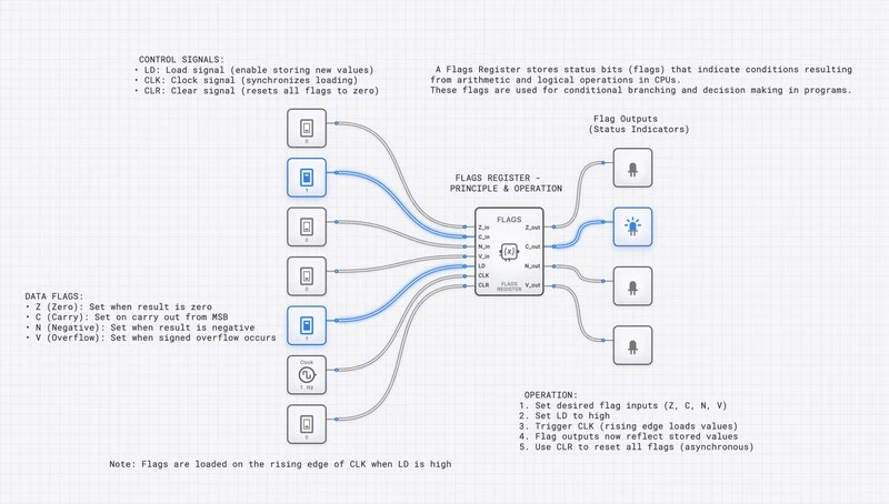
CPU Flags Register
Processor flags register with condition code inputs. Learn status flag operation in CPU design and condition testing.
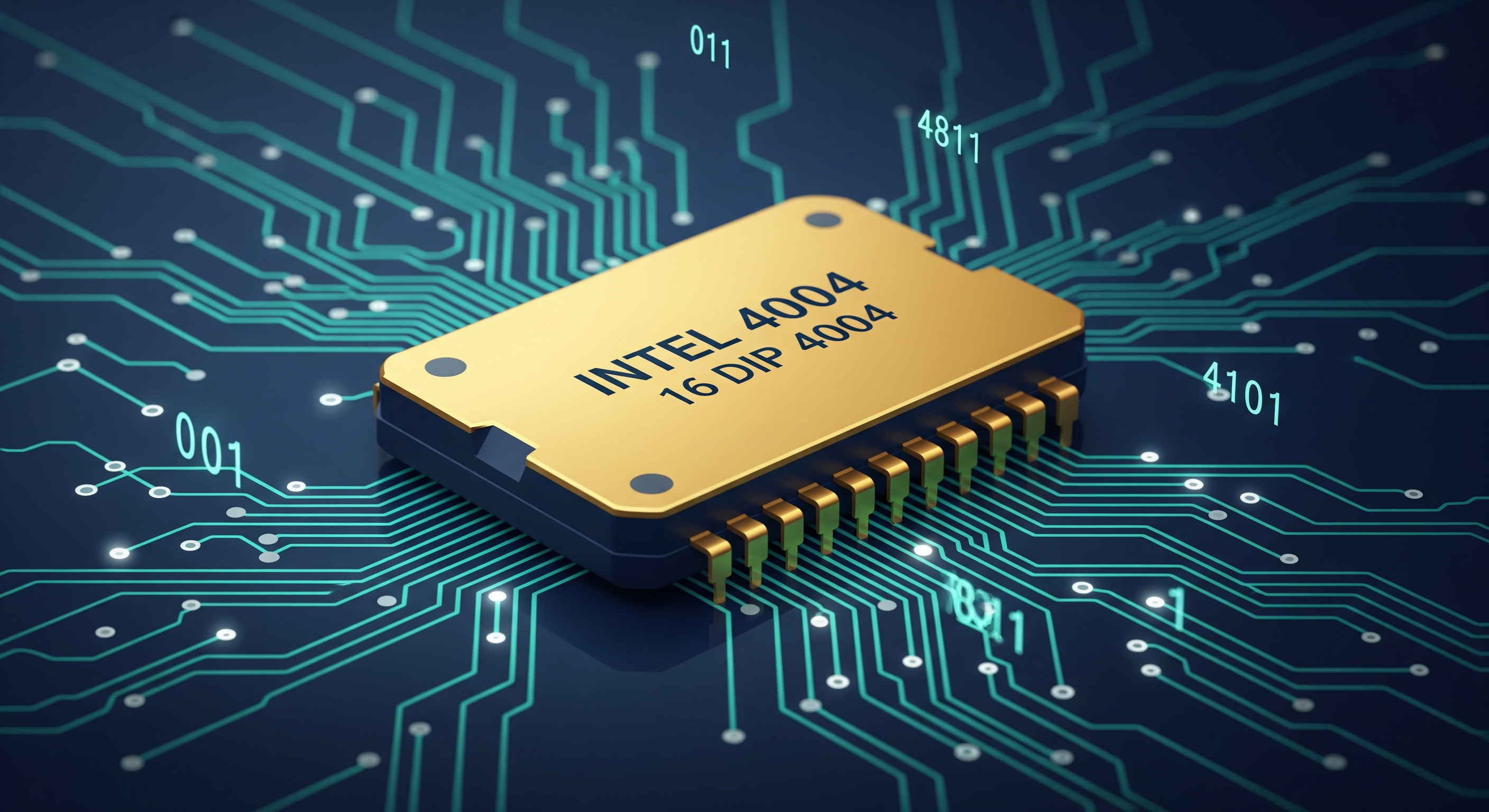
Intel 4004 — World's First Microprocessor
A working 4-bit microprocessor in the spirit of the 1971 Intel 4004 — the world's first single-chip CPU. A real stored program (4 × 3 by repeated addition) flows through FETCH → DECODE → EXECUTE → STORE on three tri-state buses, and a dedicated product display steps a clean 0 → 4 → 8 → 12 before the machine halts.
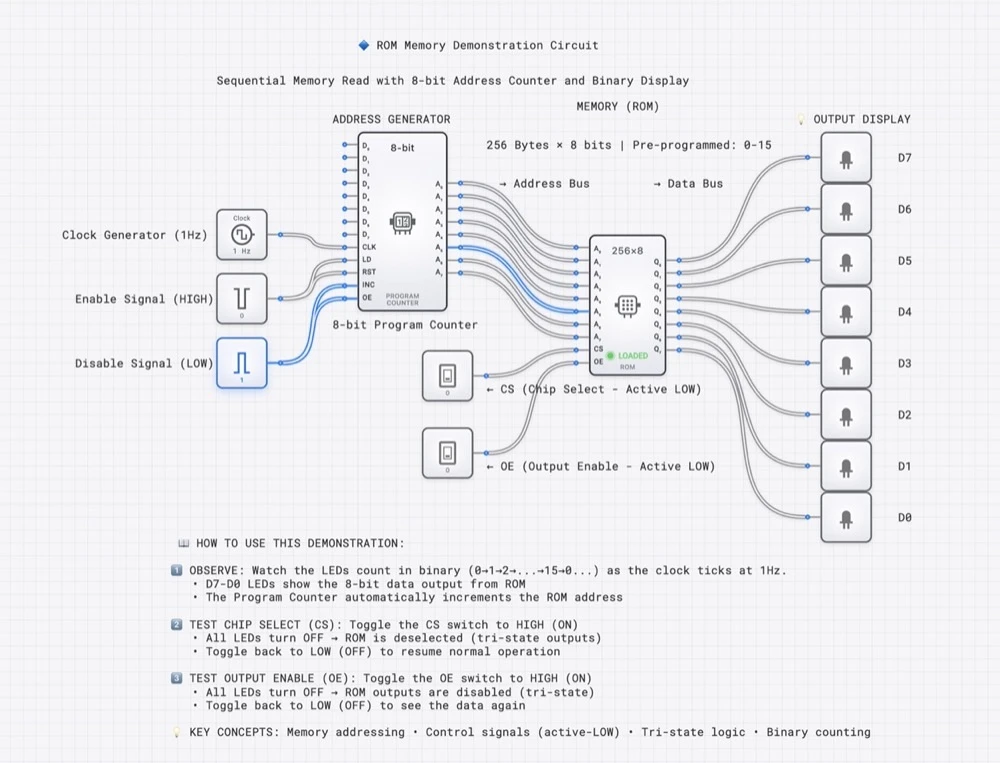
ROM Memory Demonstration Circuit
Interactive ROM memory demonstration circuit featuring sequential address generation with an 8-bit Program Counter, binary counting display (0-15), and control signal testing for Chip Select (CS) and Output Enable (OE). Ideal for learning memory addressing, tri-state logic, and active-LOW control signals.
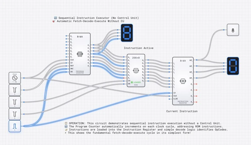
Sequential Instruction Executor
Basic CPU with program counter, ROM, and instruction register. Learn instruction fetch and execution cycles in processor design.