Logic Gates 101: A Visual Introduction to AND, OR, and NOT with DigiSim.io


Digital logic has a visual language. Gate symbols, truth tables, timing diagrams, and signal-flow schematics are the notation that engineers use to design, communicate, and debug circuits. Learning to read this visual language is as important as understanding the underlying Boolean algebra. This tutorial focuses on seeing: what each gate symbol means at a glance, how to read truth tables as visual patterns, how timing diagrams reveal behavior that static diagrams hide, and how the oscilloscope turns abstract logic into observable waveforms.
The Visual Vocabulary: Gate Symbols
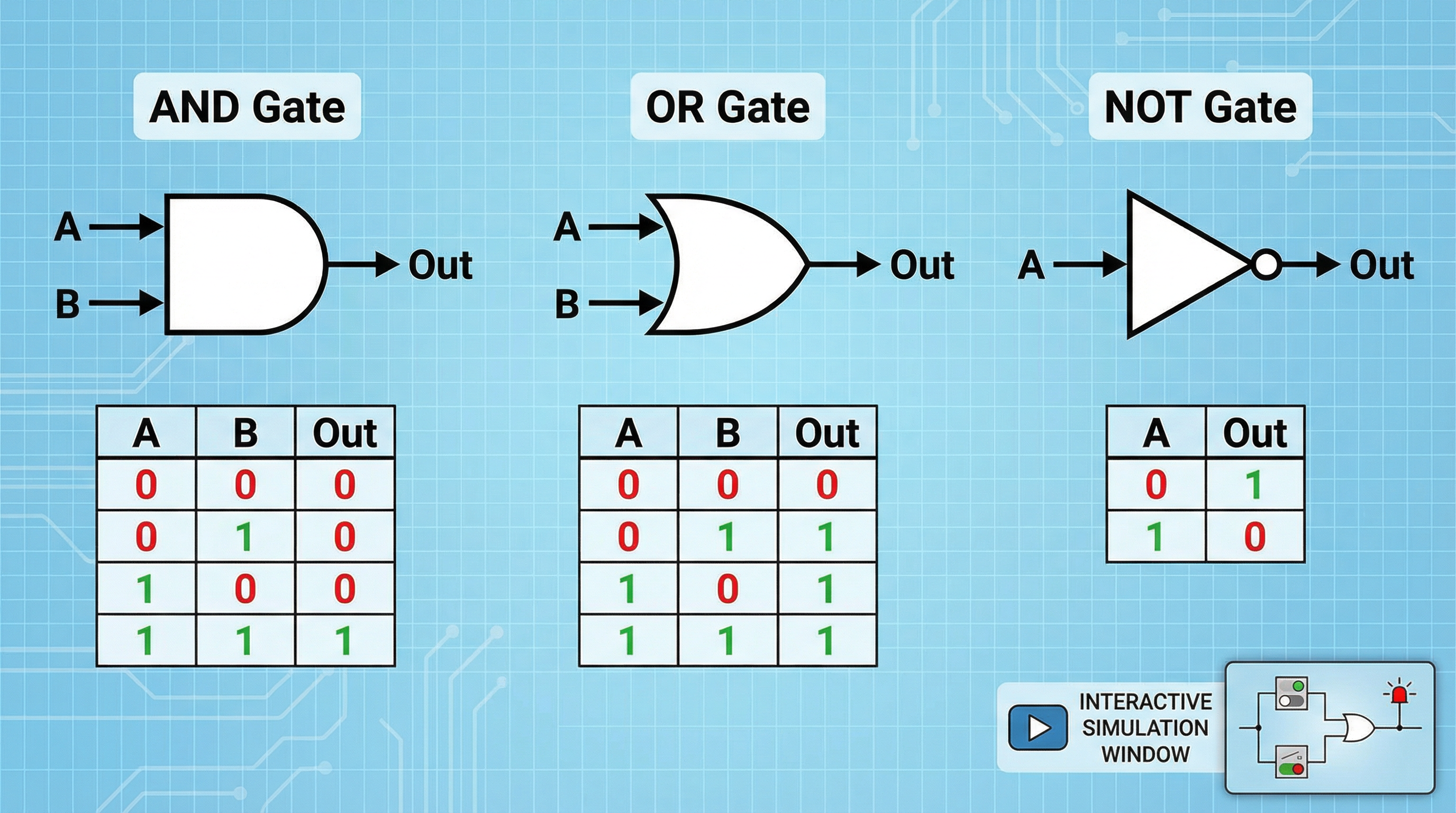
Every logic gate has a standardized symbol defined by ANSI/IEEE Std 91-1984 (the “distinctive shape” standard used in most textbooks and simulators, including DigiSim.io). Learning to recognize these shapes instantly is the first step in reading any circuit diagram.
The NOT Gate
- Symbol: A triangle pointing right with a small circle (called a bubble) at the output.
- Visual meaning: The triangle represents a buffer (signal passes through), and the bubble means “invert.” Anywhere you see a bubble on a schematic, it indicates inversion.
- Input lines: One, entering the left side of the triangle.
- Output line: One, leaving the bubble on the right.
The NOT gate is the only single-input gate you will encounter at this level. If you see a triangle-with-bubble, you know immediately: the output is the opposite of the input.
| Input (A) | Output (Y) |
|---|---|
| 0 | 1 |
| 1 | 0 |
Visual pattern to memorize: The truth table for NOT is a perfect diagonal flip. When the input column goes 0-then-1, the output column goes 1-then-0. Opposites, always.
The AND Gate
- Symbol: A flat left edge with a curved (D-shaped) right edge.
- Visual meaning: The flat edge collects inputs; the curved edge produces the output. Think of the “D” shape as a door that only opens when all inputs push together.
- Input lines: Two or more, entering the flat left side.
- Output line: One, leaving the curved right side.
| Input A | Input B | Output (Y) |
|---|---|---|
| 0 | 0 | 0 |
| 0 | 1 | 0 |
| 1 | 0 | 0 |
| 1 | 1 | 1 |
Visual pattern to memorize: In the truth table, the output column is almost entirely 0s. Only the very last row, where every input is 1, produces a 1. For a 2-input AND gate, that is 1 out of 4 rows. For a 3-input AND gate, it would be 1 out of 8. The AND gate is visually “dark” — it outputs 1 reluctantly, only under complete consensus.
The OR Gate
- Symbol: A curved left edge (concave, like a shield) with a pointed right edge.
- Visual meaning: The curved input edge “gathers” multiple signals, and any one of them is sufficient to push the output high.
- Input lines: Two or more, entering the curved left side.
- Output line: One, leaving the pointed right side.
| Input A | Input B | Output (Y) |
|---|---|---|
| 0 | 0 | 0 |
| 0 | 1 | 1 |
| 1 | 0 | 1 |
| 1 | 1 | 1 |
Visual pattern to memorize: The OR truth table is the mirror image of AND. The output column is almost entirely 1s. Only the first row, where every input is 0, produces a 0. The OR gate is visually “bright” — it defaults to 1 and only goes dark when given no reason to fire.
Recognizing Gates at a Glance
| Shape | Gate | Quick Rule |
|---|---|---|
| Triangle + bubble | NOT | Flip the input |
| Flat left, curved right (D-shape) | AND | All 1s required |
| Curved left, pointed right (shield) | OR | Any 1 sufficient |
When reading a schematic with dozens of gates, you do not parse the truth table of each one. You recognize the shape and know the rule. This pattern recognition is what “fluency” in digital logic looks like.
Reading Truth Tables as Visual Patterns
A truth table is more than a lookup chart. It is a visual fingerprint of a gate’s behavior. With practice, you can identify a gate from its truth table alone by scanning the output column.
The Output Column Tells the Story
For 2-input gates, the input columns always follow the same pattern (the binary counting sequence: 00, 01, 10, 11). The output column is what changes between gate types.
AND output column: 0, 0, 0, 1 — a single 1 at the bottom. Visually: almost all dark.
OR output column: 0, 1, 1, 1 — a single 0 at the top. Visually: almost all bright.
NAND output column: 1, 1, 1, 0 — the inverse of AND. All bright except the bottom.
NOR output column: 1, 0, 0, 0 — the inverse of OR. All dark except the top.
XOR output column: 0, 1, 1, 0 — a 1 only when inputs differ. Visually: a checkerboard pattern.
This visual approach scales. A 3-input AND gate has 8 rows with a single 1 in the last position. A 3-input OR gate has 8 rows with a single 0 in the first position. Spotting these patterns lets you verify truth tables quickly during design and debugging.
Exercise: Identify the Gate
Look at this output column for a 2-input gate: 1, 0, 0, 0. Which gate is it?
The pattern is: output is 1 only when both inputs are 0. That is the NOR gate (). The single 1 at the top is the hallmark of NOR, just as the single 1 at the bottom is the hallmark of AND.
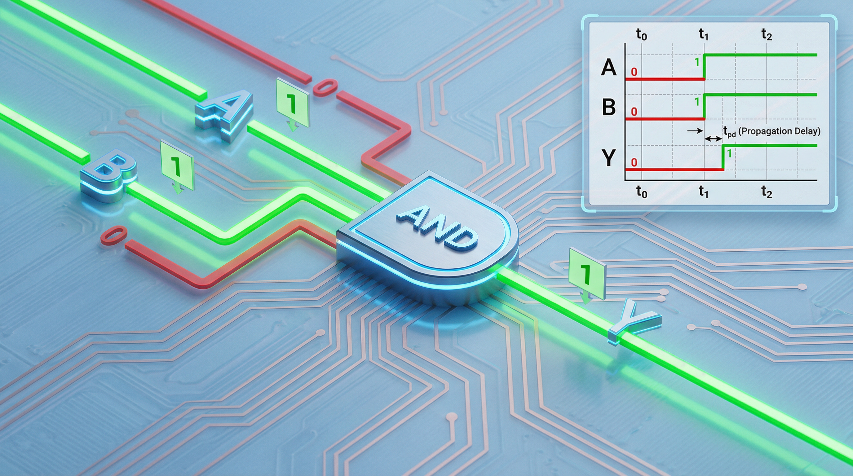
Timing Diagrams: Seeing Logic in Time
Truth tables show the static relationship between inputs and outputs: if the inputs are this, the output is that. But real circuits operate in time. Inputs change, and outputs respond. A timing diagram plots signal values (HIGH or LOW) on the vertical axis against time on the horizontal axis, showing exactly when transitions occur.
Anatomy of a Timing Diagram
A timing diagram has multiple horizontal lanes, one per signal. Each lane shows a rectangular waveform:
- HIGH is drawn at the top of the lane.
- LOW is drawn at the bottom.
- Transitions are vertical edges between the two levels.
Signals are aligned vertically so you can read any point in time by drawing a vertical line and noting the value of each signal where the line crosses.
Reading a NOT Gate Timing Diagram
Imagine a clock signal feeding a NOT gate:
- Input lane (A): A square wave alternating between 0 and 1.
- Output lane (Y): A square wave that is the exact mirror image — HIGH when A is LOW, LOW when A is HIGH.
The timing diagram makes the inversion visually obvious. Every rising edge on A corresponds to a falling edge on Y, and vice versa. This is something a truth table tells you in two rows; the timing diagram shows you it is true continuously, at every moment.
Reading an AND Gate Timing Diagram
Now imagine two signals, A and B, feeding an AND gate:
- A lane: A square wave toggling at some frequency.
- B lane: A constant HIGH signal.
- Y lane: The output follows A exactly, because .
Now change B to a constant LOW:
- Y lane: The output flatlines to 0, regardless of A, because .
This reveals the AND gate’s role as a signal gate: B acts as a control that either passes or blocks signal A. In the timing diagram, you can literally see the output waveform appear and vanish as B changes. No truth table conveys this as intuitively.
Propagation Delay Becomes Visible
In an ideal timing diagram, input and output transitions are perfectly aligned. In a real (or detailed simulation) timing diagram, the output transition lags behind the input by the propagation delay (). This appears as a small horizontal gap between the input edge and the output edge.
When you chain multiple gates in series, these gaps accumulate. A timing diagram of a 4-gate chain shows the output shifting progressively later relative to the original input. This visual shift is how engineers identify the critical path — the longest delay through a circuit — which determines the maximum operating frequency.
The Oscilloscope: Your Visual Debugging Tool
In DigiSim.io, the oscilloscope is the tool that generates timing diagrams in real time from your running circuit. It is the single most important visual tool for understanding dynamic behavior.
How to Use the Oscilloscope
- Place an oscilloscope on the canvas from the measurement components.
- Connect channels to the signals you want to observe. Connect Channel 1 to an input, Channel 2 to the gate output.
- Add a CLOCK component as a signal source. The clock provides a continuously toggling signal that makes waveforms visible on the oscilloscope.
- Run the simulation and observe the waveforms updating in real time.
Experiment 1: Visualize Inversion
- Connect a CLOCK to a NOT gate, and connect the NOT gate output to an Output Light.
- Connect oscilloscope Channel 1 to the clock signal, Channel 2 to the NOT gate output.
- Observe: the two waveforms are perfect mirror images. Every HIGH on Channel 1 corresponds to a LOW on Channel 2.
Experiment 2: Visualize Signal Gating
- Connect a CLOCK to one input of an AND gate.
- Connect an Input Switch to the other input.
- Connect the AND gate output to an Output Light and oscilloscope Channel 2. Connect the clock to Channel 1.
- With the switch ON (1): the output waveform on Channel 2 matches the clock on Channel 1. The AND gate passes the signal.
- Flip the switch OFF (0): the output waveform flatlines to LOW. The AND gate blocks the signal.
Toggle the switch back and forth and watch the output waveform appear and disappear. This is clock gating, a technique used in every modern processor to save power by disabling the clock to idle circuit blocks.
Experiment 3: Visualize OR Combination
- Connect two CLOCK components running at different frequencies to the two inputs of an OR gate.
- Connect the OR output to oscilloscope Channel 3, and the two clocks to Channels 1 and 2.
- Observe: the output is HIGH whenever either input is HIGH. The output waveform is the visual “union” of the two input waveforms — it is LOW only during the intervals where both inputs happen to be LOW simultaneously.
This visual demonstration makes the OR gate’s behavior intuitive in a way that no static truth table can.
Reading Circuit Schematics: Signal Flow
A circuit schematic is a map. Learning to read it means learning its conventions:
Flow Direction
Signals flow left to right by convention. Inputs are on the left side of the page, outputs on the right. When you encounter a schematic, start reading from the left (where the input switches or external signals are) and trace the signal rightward through successive gates to the output.
Wire Conventions
- Connected wires are shown with a dot at the junction. If two wires cross and there is a dot, they are electrically connected.
- Unconnected crossings have no dot. The wires just pass over each other.
- Bus notation groups multiple related wires (like an 8-bit data bus) into a single thick line with a label, reducing visual clutter.
Labeling
Professional schematics label inputs (A, B, C or descriptive names like ENABLE, DATA, CLOCK) and outputs (Y, Q, SUM, CARRY). Always label your inputs and outputs in DigiSim.io using the text tool. A circuit without labels is like code without variable names.
Hierarchical Design
Complex circuits are decomposed into subcircuits. A schematic might show a “Full Adder” as a single box with labeled inputs (A, B, Cin) and outputs (Sum, Cout). Inside that box is a network of AND, OR, and XOR gates. This hierarchical decomposition is how engineers manage complexity: each level of the hierarchy can be read and understood independently.
Visual Patterns in Combined Circuits
As you progress beyond individual gates, recognizing visual patterns in gate combinations accelerates your understanding.
The Inverter Bubble Chain
When you see a NAND gate (AND symbol + bubble) feeding into another gate with a bubble on its input, the two bubbles cancel out. This is De Morgan’s theorem made visual: . Experienced engineers spot bubble cancellation instantly, simplifying their mental model of the circuit.
The XOR Pattern
An XOR gate can be built from AND, OR, and NOT gates:
In a schematic, this appears as two AND gates, each fed by one original input and the inverse of the other, with their outputs combined in an OR gate. Once you recognize this pattern, you can identify XOR logic even when it is not drawn as a single XOR symbol.
The Multiplexer Pattern
A 2-to-1 multiplexer selects between two data inputs based on a select signal:
Visually: two AND gates, each gating one data input with the select signal (one inverted, one not), feeding into an OR gate. This pattern appears everywhere — in ALUs, memory addressing, and data routing — and recognizing it visually is a core skill.
Putting It All Together: A Visual Workflow
The visual workflow for understanding any digital circuit:
- Read the schematic left to right. Identify inputs, trace signal flow, note gate types by their shapes.
- Build the truth table. For each combination of inputs, trace the signal through each gate and record the output.
- Verify with simulation. Build the circuit in DigiSim.io, toggle switches through all input combinations, and confirm the truth table.
- Observe timing with the oscilloscope. Replace manual switches with clock sources and watch the dynamic behavior. Look for propagation delay and signal gating effects.
- Debug visually. If the output is wrong, connect the oscilloscope to intermediate nodes (the outputs of internal gates) to find where the signal diverges from expectation.
This workflow applies whether you are debugging a single gate or a multi-stage arithmetic circuit. The visual tools — symbols, truth tables, timing diagrams, and the oscilloscope — are the instruments that make abstract logic tangible.
Next Steps
With the visual language of digital logic internalized, you are ready to:
- Build combined circuits (NAND, NOR, XOR) and recognize their visual patterns in larger designs.
- Read and draw timing diagrams for multi-gate circuits, identifying propagation delay and critical paths.
- Use the oscilloscope as your primary debugging tool for any circuit in DigiSim.io.
- Design hierarchically, building small verified subcircuits and combining them into larger systems.
The goal is not to memorize every truth table. The goal is to reach the point where you glance at a gate symbol and know its behavior, look at an output waveform and know which gate produced it, and trace a schematic from input to output as naturally as reading a sentence.
That is visual fluency in digital logic.