Demystifying Digital Logic: Your First Steps with AND, OR, and NOT Gates on DigiSim.io

Most tutorials on logic gates tell you what each gate does. This one explains why it works that way. We will trace the path from raw physics — how electrons move through transistors — up through the CMOS circuits that implement NOT, OR, and AND gates in every modern chip. If you have already seen the truth tables and want to understand the engineering beneath them, this is where that understanding starts.
From Sand to Switches: How Transistors Work
Every logic gate is built from transistors, and every transistor is built from silicon. Pure silicon is a poor conductor, but by introducing trace amounts of other elements (a process called doping), engineers create two types of semiconductor material:
- n-type silicon has extra electrons, making it easy for negative charge to flow.
- p-type silicon has “holes” (missing electrons), making it easy for positive charge to flow.
A MOSFET (Metal-Oxide-Semiconductor Field-Effect Transistor) sandwiches a thin insulating oxide layer between a metal gate terminal and a channel of doped silicon. Applying voltage to the gate terminal creates an electric field across the oxide, which either attracts or repels charge carriers in the channel, switching it between conducting and non-conducting states.
There are two complementary types:
- NMOS transistor — Conducts when the gate voltage is HIGH. Think of it as a switch that closes when you apply voltage.
- PMOS transistor — Conducts when the gate voltage is LOW. It is the mirror image: the switch closes when voltage is removed.
This complementary pairing is the foundation of CMOS (Complementary Metal-Oxide-Semiconductor) technology, which has dominated chip manufacturing since the 1980s.
Why CMOS? The Power Argument
Before CMOS, chips used NMOS-only logic. The problem: NMOS-only circuits consume power continuously, even when idle, because current flows through resistive pull-up elements regardless of the output state. CMOS solves this by pairing each NMOS transistor with a PMOS transistor arranged so that in every stable state, one transistor is off, blocking the path from power supply to ground. Current flows only during the brief instant of switching. This is why your phone’s processor can contain billions of transistors without immediately melting.
The key design rule of CMOS: in every logic gate, a pull-up network of PMOS transistors connects the output to the supply voltage (), and a pull-down network of NMOS transistors connects the output to ground (). The two networks are complementary — when one conducts, the other does not.
The NOT Gate: CMOS Implementation
The NOT gate (inverter) is the simplest CMOS circuit, requiring exactly one PMOS and one NMOS transistor.
Circuit Structure
- The PMOS transistor connects to the output. It conducts when the input is LOW.
- The NMOS transistor connects the output to . It conducts when the input is HIGH.
- Both gate terminals are tied to the input signal.
How It Works, Physically
When input = 0 (LOW): The PMOS transistor turns on (PMOS conducts on low gate voltage), connecting the output to . The NMOS transistor turns off, disconnecting the output from ground. Result: output is pulled HIGH. Output = 1.
When input = 1 (HIGH): The NMOS transistor turns on, connecting the output to ground. The PMOS transistor turns off, disconnecting the output from . Result: output is pulled LOW. Output = 0.
In both states, there is no direct path from to . This is the CMOS efficiency advantage: zero static power dissipation.
| Input (A) | PMOS State | NMOS State | Output (Y) |
|---|---|---|---|
| 0 | ON | OFF | 1 |
| 1 | OFF | ON | 0 |
Boolean expression:
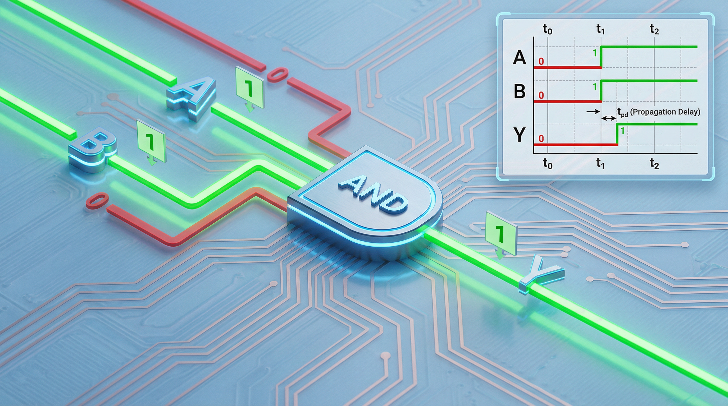
Propagation Delay in the Inverter
The output does not change the instant the input changes. The MOSFET gate terminal has parasitic capacitance — the oxide layer between the gate and the channel acts as a tiny capacitor. Charging or discharging this capacitance takes time. Additionally, the output node itself has capacitance from wiring and the input capacitance of downstream gates.
The propagation delay of a CMOS inverter is approximately:
where is the effective on-resistance of the conducting transistor and is the total capacitance at the output node. In a modern 5nm process, this delay is in the range of a few picoseconds per gate. But when millions of gates are chained together, these delays define the maximum clock frequency of the entire chip.
The NAND Gate: CMOS Implementation
Before building AND and OR gates, we need to understand NAND and NOR, because in CMOS technology, NAND and NOR are the native gate types. AND and OR gates are always implemented as NAND or NOR followed by an inverter.
A 2-input CMOS NAND gate uses two PMOS transistors in parallel (pull-up network) and two NMOS transistors in series (pull-down network).
How It Works
- The output is pulled LOW only when both NMOS transistors conduct, which requires both inputs to be HIGH. (This is the AND condition, inverted at the output.)
- If either input is LOW, at least one PMOS transistor conducts, pulling the output HIGH.
| Input A | Input B | Pull-Up (PMOS) | Pull-Down (NMOS) | Output (Y) |
|---|---|---|---|---|
| 0 | 0 | Both ON | Both OFF | 1 |
| 0 | 1 | A’s PMOS ON | Series broken | 1 |
| 1 | 0 | B’s PMOS ON | Series broken | 1 |
| 1 | 1 | Both OFF | Both ON | 0 |
Boolean expression:
Why NAND Is “Native”
The series NMOS pull-down and parallel PMOS pull-up emerge naturally from the CMOS design rules. An AND gate, by contrast, requires a NAND gate followed by an inverter — that means four NMOS and four PMOS transistors instead of two and two. This is why NAND gates are faster, smaller, and consume less power than AND gates in CMOS. It is also why NAND is called the “universal gate”: any Boolean function can be expressed using only NAND gates, and since NAND is the cheapest gate to fabricate in CMOS, real chips are overwhelmingly NAND-based.
The AND Gate: Why It Is NOT Native
Given what we now know about CMOS, the AND gate is simply a NAND gate with its output fed through an inverter:
This means a 2-input AND gate requires four transistors for the NAND plus two transistors for the inverter = six transistors total. Compared to the NAND gate’s four transistors, the AND gate is 50% larger and slightly slower due to the extra inverter stage adding propagation delay.
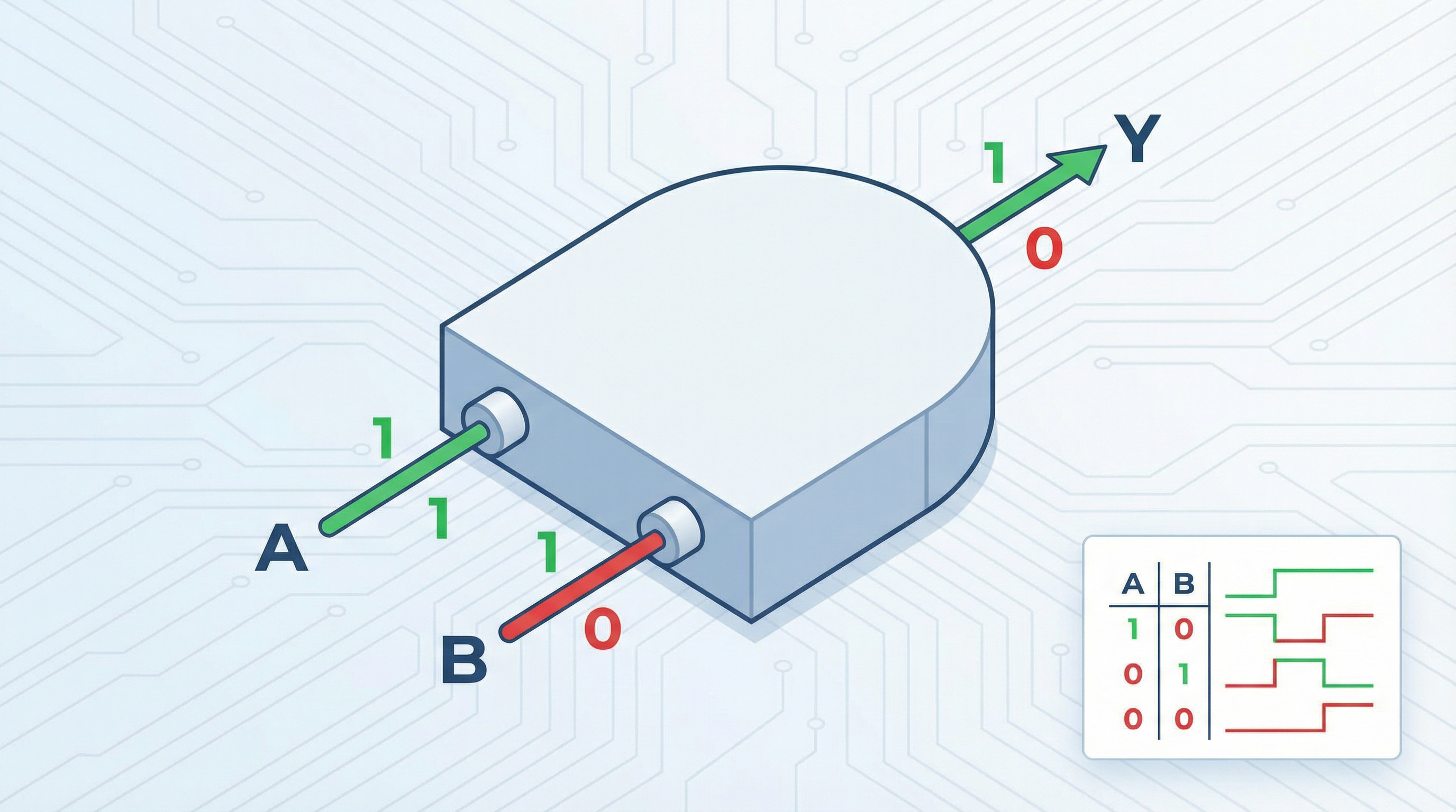
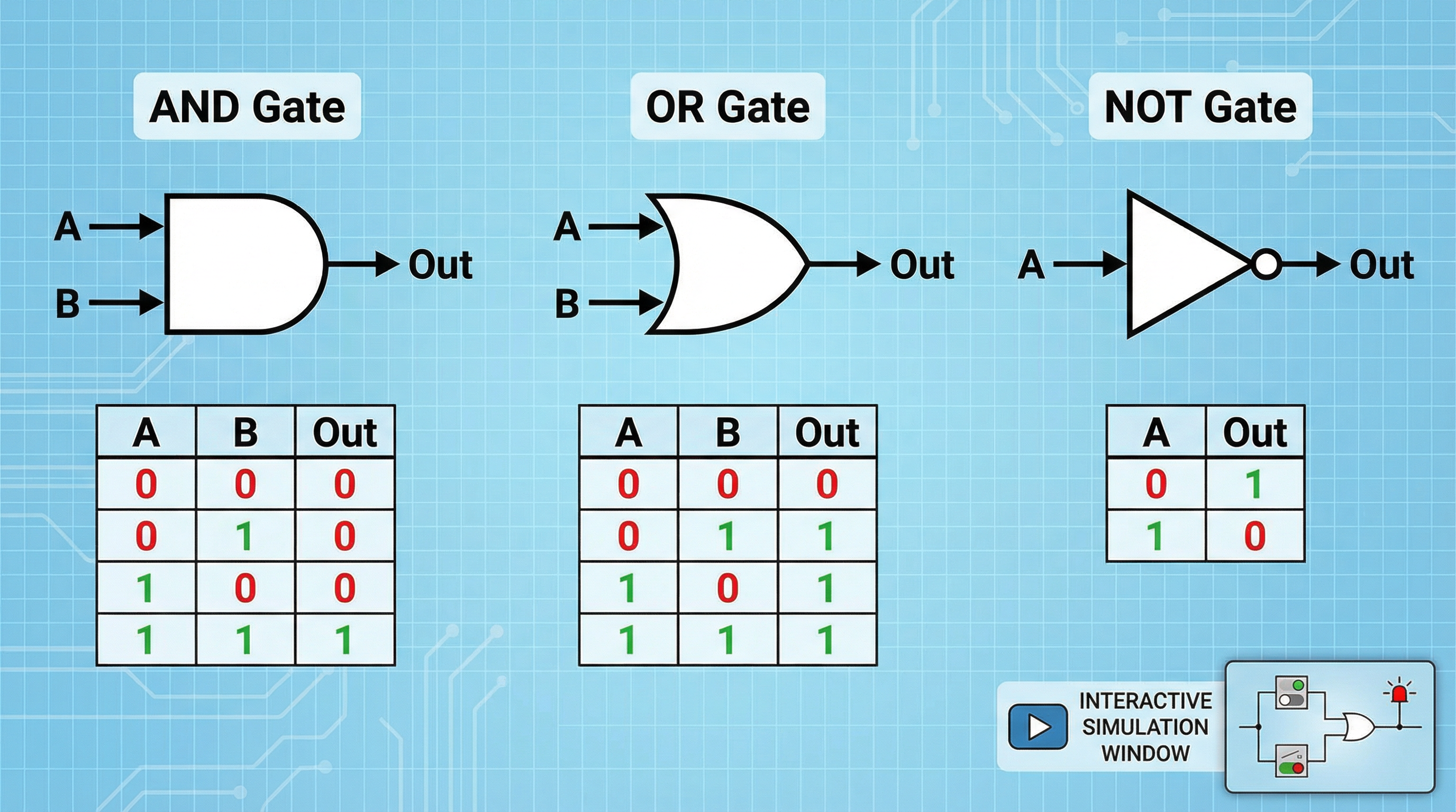
| Input A | Input B | Output (Y) |
|---|---|---|
| 0 | 0 | 0 |
| 0 | 1 | 0 |
| 1 | 0 | 0 |
| 1 | 1 | 1 |
Boolean expression:
The practical takeaway: when you see an AND gate in a schematic, know that the silicon underneath implements it as NAND + NOT. Circuit optimizers often eliminate redundant inversions to reduce transistor count. If a signal feeds into a gate that will invert it anyway, the optimizer removes the intermediate inverter, saving area and delay.
The NOR Gate: CMOS Implementation
The NOR gate is the NAND gate’s dual. It uses two PMOS transistors in series (pull-up) and two NMOS transistors in parallel (pull-down).
How It Works
- The output is pulled HIGH only when both PMOS transistors conduct, which requires both inputs to be LOW.
- If either input is HIGH, at least one NMOS transistor conducts, pulling the output LOW.
| Input A | Input B | Output (Y) |
|---|---|---|
| 0 | 0 | 1 |
| 0 | 1 | 0 |
| 1 | 0 | 0 |
| 1 | 1 | 0 |
Boolean expression:
Like NAND, NOR is also a universal gate: any Boolean function can be built from NOR gates alone. However, in practice, NAND gates are preferred over NOR gates because PMOS transistors have lower carrier mobility than NMOS transistors. Series PMOS (as in NOR) is slower than series NMOS (as in NAND), so NAND gates are inherently faster in CMOS technology.
The OR Gate: Also Not Native
The OR gate is implemented as NOR + inverter:
Six transistors total, same as the AND gate. Same penalty in area and delay relative to the native NOR.
| Input A | Input B | Output (Y) |
|---|---|---|
| 0 | 0 | 0 |
| 0 | 1 | 1 |
| 1 | 0 | 1 |
| 1 | 1 | 1 |
Boolean expression:
De Morgan’s Theorem: The Bridge Between AND and OR
At the transistor level, the relationship between AND/NAND and OR/NOR becomes visually obvious. A NAND gate (parallel PMOS, series NMOS) produces the opposite truth table pattern from a NOR gate (series PMOS, parallel NMOS). De Morgan’s theorems formalize this duality:
The first theorem says: a NAND gate is equivalent to an OR gate with inverted inputs. The second says: a NOR gate is equivalent to an AND gate with inverted inputs.
This is not just a mathematical curiosity. Circuit designers use De Morgan’s laws constantly to convert between gate types, reducing the number of transistors needed or improving timing on critical paths. When you see a professional schematic, the choice between a NAND symbol and an OR-with-bubbles symbol is often a deliberate communication about the designer’s intent.
Power, Speed, and Area: The Tradeoffs
Every gate design involves three competing constraints:
Static Power
CMOS gates consume essentially zero static power because one of the two networks (pull-up or pull-down) is always off. Leakage current through the off transistors does exist and becomes significant at nanometer scales, but it is orders of magnitude smaller than the static power of older technologies.
Dynamic Power
Every time a gate switches, it charges or discharges the load capacitance, consuming energy proportional to . The total dynamic power of a chip is:
where is the activity factor (fraction of gates switching per cycle), is total switched capacitance, is supply voltage, and is clock frequency. This equation explains why reducing supply voltage (even slightly) dramatically reduces power: the relationship is quadratic.
Propagation Delay
As discussed, each gate contributes a propagation delay. The critical path (longest chain of gates from input to output) determines the maximum clock frequency. Larger transistors switch faster (lower ) but consume more area and more power. Smaller transistors save area and power but are slower. This is the fundamental tension in chip design.
Area
Each transistor occupies physical space on the die. A chip with fewer transistors per gate can fit more gates, enabling more complex designs. This is another reason NAND (4 transistors) is preferred over AND (6 transistors) in real implementations.
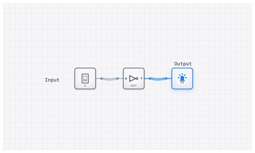
Observing Gate Behavior in Simulation
While digisim.io operates at the logical level rather than the transistor level, it faithfully represents the input-output relationships we have derived from the physics. Using the OSCILLOSCOPE, you can observe:
- The NOT gate cleanly inverting a clock signal.
- The AND gate passing or blocking a signal based on a control input.
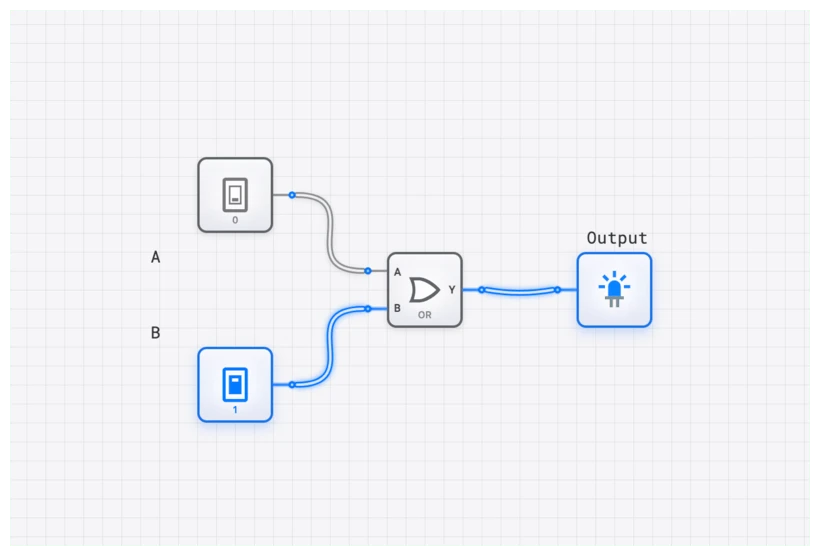
- The OR gate combining multiple trigger sources into a single output.
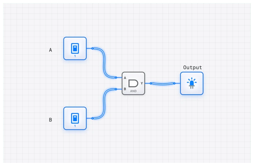
Connect a CLOCK to one input of an AND gate, a manual INPUT_SWITCH to the other, and an oscilloscope channel to the output. Toggle the switch and watch the output waveform appear and disappear. You are watching, at a logical level, the same NMOS-series-path-completing behavior that occurs at the transistor level.
A Brief History: From Relays to CMOS
Understanding why gates look the way they do requires a brief look at how we got here:
- 1937 — Claude Shannon’s thesis shows that Boolean algebra maps to relay circuits, founding digital logic as a discipline.
- 1947 — Bardeen, Brattain, and Shockley invent the transistor at Bell Labs, replacing mechanical relays with solid-state switches.
- 1958 — Jack Kilby demonstrates the first integrated circuit, putting multiple transistors on a single chip.
- 1963 — Frank Wanlass at Fairchild Semiconductor patents CMOS, though it would not become dominant for two decades.
- 1971 — Intel 4004, the first commercial microprocessor, uses PMOS technology with about 2,300 transistors.
- 1985 — CMOS becomes the dominant fabrication technology as its power advantages outweigh its initially higher manufacturing cost.
- 2020s — Modern processors contain over 100 billion transistors, virtually all implemented in CMOS, at process nodes of 3-5 nanometers.
Every generation has shrunk the transistors, increased the count, and raised the clock frequency, but the fundamental CMOS gate structures — the complementary pull-up and pull-down networks — remain recognizably the same as Wanlass’s 1963 patent.
Key Takeaways
- Logic gates are transistor circuits. Every AND, OR, and NOT gate is implemented as a specific arrangement of PMOS and NMOS transistors.
- NAND and NOR are the native CMOS gates. AND and OR require an extra inverter stage, making them larger and slower.
- CMOS achieves near-zero static power by ensuring that in every stable state, either the pull-up or pull-down network is off.
- Propagation delay is real and consequential. It emerges from parasitic capacitance at the transistor level and limits the maximum clock frequency.
- De Morgan’s theorems are not just algebraic identities; they reflect the physical duality between NAND and NOR implementations.
The truth tables are where most tutorials stop. The transistor-level understanding is where engineering begins.