Digital Logic 101: Your First Steps with AND, OR, and NOT Gates
AND, OR, and NOT are the three fundamental logic gates. This beginner's guide builds each from scratch and combines them into a NAND in your browser.

TL;DR: AND, OR, and NOT are the three fundamental logic gates. AND outputs 1 only when all inputs are 1; OR outputs 1 when any input is 1; NOT inverts a single input. Combining them produces NAND, the universal gate from which every other digital circuit can be built.
The fastest way to learn digital logic is to build circuits. Reading truth tables is useful, but toggling switches and watching outputs change is where intuition forms. This tutorial walks you through building each of the three fundamental logic gates — NOT, AND, and OR — step by step in digisim.io. Every section ends with a working circuit you built yourself.
No prerequisites. No installations. Open a browser tab to digisim.io and follow along.
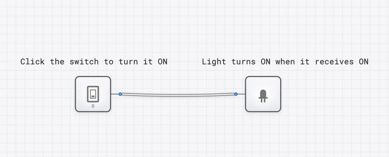
Before You Start: The Switch-to-Light Circuit
Every digital circuit has inputs and outputs. In digisim.io, the basic input is an INPUT_SWITCH (click to toggle between 0 and 1) and the basic output is an OUTPUT_LIGHT (glows when receiving a 1). Before touching any gates, build this minimal circuit to get comfortable with the interface.
Build it:
- Open digisim.io/circuits/new.
- From the component palette, drag an Input Switch onto the canvas.
- Drag an Output Light to the right of it.
- Click the output node (small circle) on the switch and drag to the input node on the light. A wire appears.
- Click the switch to toggle it. The light follows: ON when the switch is 1, OFF when it is 0.
This confirms the fundamental idea: a digital signal flows from source to destination through a wire. Every circuit you build from here adds logic between the source and destination.
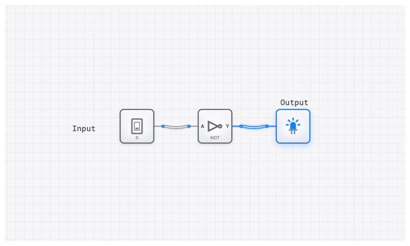
1. Build a NOT Gate Circuit (The Inverter)
The NOT gate takes a single input and flips it. Input 1 produces output 0. Input 0 produces output 1. It is the simplest gate, and building it first gives you confidence with the wiring workflow.
Step-by-Step Build
- Place the input. Drag an Input Switch onto the left side of the canvas.
- Place the gate. Drag a NOT Gate from the Logic Gates section and position it to the right of the switch.
- Place the output. Drag an Output Light to the right of the NOT gate.
- Wire input to gate. Click the switch’s output node and drag to the NOT gate’s input node.
- Wire gate to output. Click the NOT gate’s output node and drag to the light’s input node.
- Test every input combination. There are only two:
| Input (A) | Expected Output (Y) | What You Should See |
|---|---|---|
| 0 | 1 | Switch OFF, Light ON |
| 1 | 0 | Switch ON, Light OFF |
Boolean expression:
What You Learned
- The NOT gate has exactly one input and one output.
- It always produces the opposite of its input.
- The small circle (bubble) on the gate symbol indicates inversion. You will see this bubble reappear on NAND and NOR gates later.
Practical Application: Active-Low Reset Lines
In microcontrollers and processors, reset pins are often “active low,” meaning the chip resets when the pin is pulled to 0. A NOT gate lets a designer convert a “press button = 1” signal into the active-low signal the chip expects. This pattern appears in virtually every embedded system.
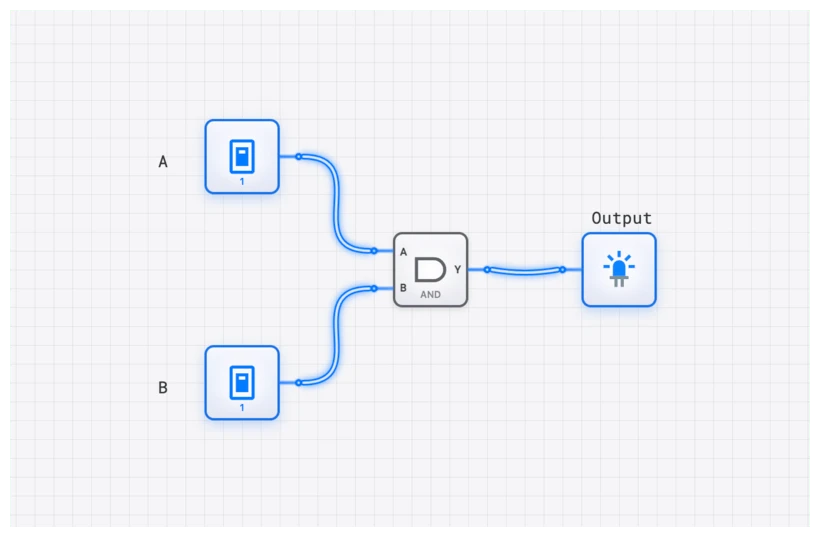
2. Build an AND Gate Circuit (The Gatekeeper)
The AND gate outputs 1 only when all inputs are 1. With two inputs, there are four possible combinations, and only one produces a 1 output. This makes the AND gate the natural choice for situations where multiple conditions must be satisfied simultaneously.
Step-by-Step Build
- Place two Input Switches on the left side of the canvas, one above the other. These are your inputs A and B.
- Place an AND Gate to the right, centered between the two switches.
- Place an Output Light to the right of the AND gate.
- Wire Switch A to the top input of the AND gate.
- Wire Switch B to the bottom input of the AND gate.
- Wire the AND gate’s output to the light.
- Systematically test all four combinations. Work through the truth table row by row:
| Input A | Input B | Expected Output (Y) | What You Should See |
|---|---|---|---|
| 0 | 0 | 0 | Both OFF, Light OFF |
| 0 | 1 | 0 | Only B ON, Light OFF |
| 1 | 0 | 0 | Only A ON, Light OFF |
| 1 | 1 | 1 | Both ON, Light ON |
Boolean expression:
The AND operation behaves like multiplication: any zero in the inputs forces the output to zero.
What You Learned
- The AND gate requires unanimity. Every input must agree on 1 for the output to be 1.
- With inputs, an AND gate has possible input combinations, but only one produces a 1 output.
- Testing all combinations systematically (not randomly) is how engineers verify correctness.
Common Pitfall: Floating Inputs
If you leave an AND gate input unconnected, you have a floating input. In physical circuits, floating inputs pick up electromagnetic noise and behave unpredictably. In digisim.io, the simulator handles this gracefully, but the habit of always connecting every pin matters when you move to real hardware. Use a CONSTANT component set to 0 or 1 if you need a fixed input value.
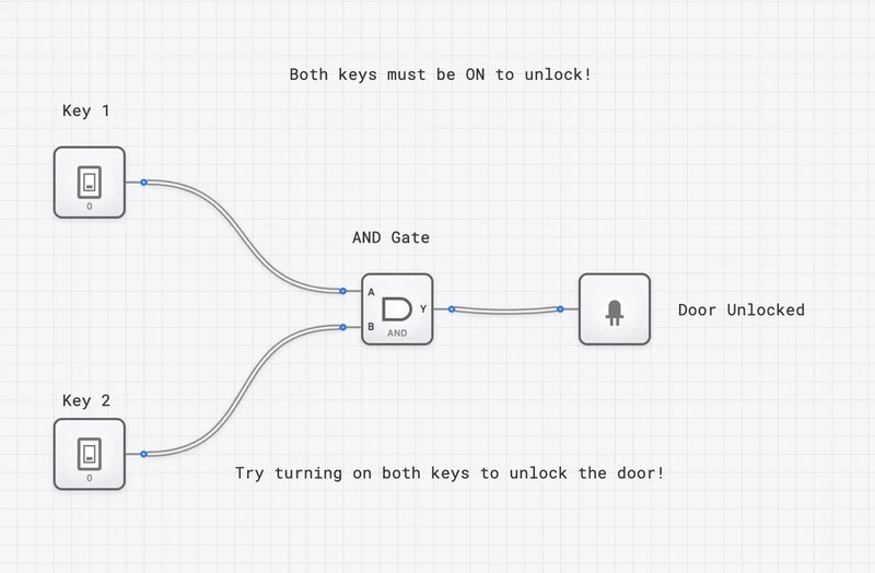
Practical Application: Two-Key Security System
The AND gate naturally models any system requiring simultaneous authorization. A bank vault needing two keys turned at once, a nuclear launch system requiring two officers, or a web application requiring both a password and a hardware token — all implement AND logic.
3. Build an OR Gate Circuit (The Inclusive Trigger)
The OR gate outputs 1 when at least one input is 1. It only outputs 0 when every input is 0. Where the AND gate enforces “all conditions required,” the OR gate enforces “any condition sufficient.”
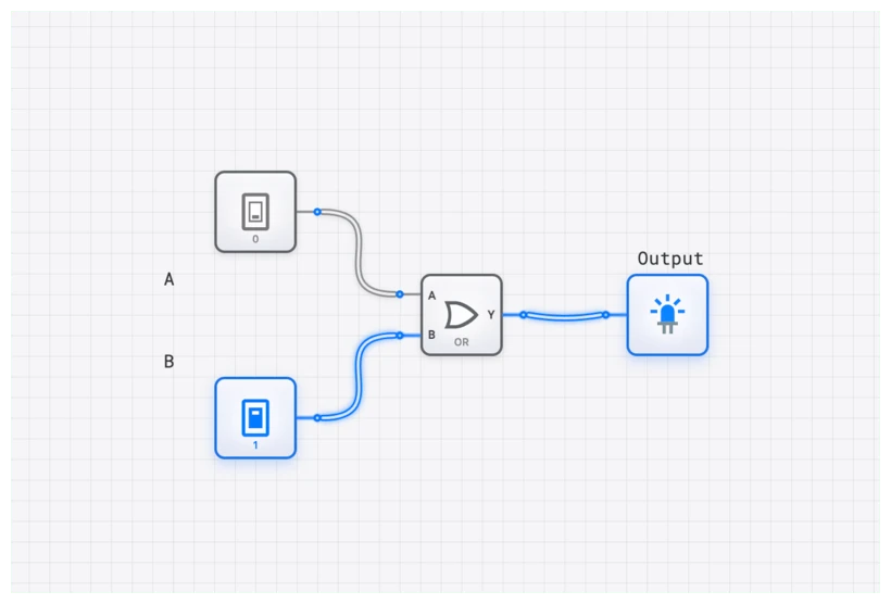
Step-by-Step Build
- Place two Input Switches on the left.
- Place an OR Gate in the center.
- Place an Output Light on the right.
- Wire Switch A to the top input of the OR gate.
- Wire Switch B to the bottom input of the OR gate.
- Wire the OR gate’s output to the light.
- Test all four combinations:
| Input A | Input B | Expected Output (Y) | What You Should See |
|---|---|---|---|
| 0 | 0 | 0 | Both OFF, Light OFF |
| 0 | 1 | 1 | Only B ON, Light ON |
| 1 | 0 | 1 | Only A ON, Light ON |
| 1 | 1 | 1 | Both ON, Light ON |
Boolean expression:
Note: this is logical OR, not arithmetic addition. In Boolean algebra, , because the output is already as HIGH as it can be.
What You Learned
- The OR gate needs only one input to be 1 for the output to fire.
- Three of the four input combinations produce a 1 output (contrast this with AND, where only one of four does).
- The OR gate is the dual of the AND gate. De Morgan’s theorem formalizes this duality: .
Practical Application: Emergency Stop Systems
Factory floors place emergency stop buttons at multiple stations around a machine. If any button is pressed, the machine must halt. This is OR logic: Button_1 OR Button_2 OR Button_3 = STOP. Adding more buttons simply adds more inputs to the OR gate.
4. Combine All Three: Build an Enable Circuit
Now that you have built each gate individually, combine them into a circuit that demonstrates how gates work together. We will build an inverted enable circuit: a data signal passes through to the output only when an enable switch is ON, and the output is inverted.
Step-by-Step Build
- Place two Input Switches. Label one “Data” and the other “Enable” using the text tool.
- Place an AND Gate to the right.
- Place a NOT Gate after the AND gate.
- Place an Output Light at the end.
- Wire: Data switch to AND input A. Enable switch to AND input B. AND output to NOT input. NOT output to Light.
- Test the behavior:
- Set Enable = 0. Toggle Data between 0 and 1. The light stays ON regardless (because the AND output is always 0, and the NOT inverts it to 1).
- Set Enable = 1. Now toggle Data. When Data = 0, the AND outputs 0, the NOT outputs 1, and the light is ON. When Data = 1, the AND outputs 1, the NOT outputs 0, and the light is OFF.
Boolean expression for this circuit:
You have just built a NAND gate from discrete AND and NOT components. The NAND gate is one of the most important gates in digital design. It is functionally complete on its own, meaning every other gate (AND, OR, NOT, XOR) can be constructed using only NAND gates.
What You Learned
- Gates can be chained: the output of one gate feeds directly into the input of another.
- Combining AND and NOT produces NAND, the universal gate.
- Complex behavior emerges from simple, composable building blocks.
5. Verify Timing with the Oscilloscope
Static tests (toggle a switch, check the light) confirm logical correctness. But digital circuits operate in time, and understanding timing behavior separates functional designs from reliable ones.
The OSCILLOSCOPE in digisim.io lets you see how signals change over time, plotted as waveforms.
Step-by-Step Build
- Start with the AND gate circuit you built in Section 2.
- Replace one of the Input Switches with a CLOCK component. The clock automatically alternates between 0 and 1 at a fixed frequency.
- Keep the other Input Switch as a manual control.
- Add an OSCILLOSCOPE to the canvas.
- Connect one oscilloscope channel to the clock output (the rapidly toggling signal).
- Connect another channel to the AND gate output.
- Set the manual switch to 1 and observe: the oscilloscope shows the clock waveform on one channel and the AND gate output on another. They should match, because the AND gate passes the clock signal through when the other input is 1.
- Now flip the manual switch to 0. The AND gate output flatlines to 0, regardless of the clock. You have just used the AND gate as a signal gate, blocking a clock signal on command.
This is the conceptual basis of clock gating in real processors. Production designs do not actually use a plain AND gate for this — the enable signal can change mid-pulse and produce a glitch on the clock. Real silicon uses an integrated clock-gating cell (an ICG): a latch that traps the enable until the clock is low, followed by an AND. The end behavior is identical to what you just demonstrated, but glitch-free. The point stands: when a functional unit is idle, its clock is gated off, stopping unnecessary switching and saving energy.
What You Learned
- The oscilloscope reveals behavior that a static light cannot: timing relationships, propagation delay, and signal gating.
- An AND gate can serve as a controllable pass/block for any digital signal.
- Clock gating is a real power-saving technique in processor design, and you just demonstrated its core mechanism.
Quick Reference: The Three Gates at a Glance
| Gate | Inputs | Output Rule | Boolean Expression | Key Use |
|---|---|---|---|---|
| NOT | 1 | Invert | Signal inversion, active-low logic | |
| AND | 2+ | All must be 1 | Conditional enable, masking | |
| OR | 2+ | Any can be 1 | Multi-source triggering |
Next Steps
You now have hands-on experience with the three fundamental gates. From here, the natural progression is:
- NAND and NOR gates — You already built a NAND in Section 4. The NOR gate is an OR followed by NOT. Both are universal gates.
- XOR gate — Outputs 1 when inputs differ. Try building it from AND, OR, and NOT gates as a challenge.
- Half adder — Combine an XOR and an AND gate to add two single-bit numbers. This is the first step toward arithmetic circuits.
- Full adder — Chain half adders to handle carry bits, enabling multi-bit addition.
Each of these builds directly on the skills you practiced today. The key principle remains the same: place components, wire them, test systematically, and verify with the oscilloscope when timing matters.
Continue by reading the AND gate component reference, or jump to the next building block — the half adder.