RAM (Memoria de acceso aleatorio)
Descripcion general
- Proposito: La RAM (memoria de acceso aleatorio) es un componente de almacenamiento digital volatil que permite leer o escribir datos en cualquier ubicacion de memoria con el mismo tiempo de acceso. Almacena temporalmente datos e instrucciones que son utilizados activamente por los sistemas digitales.
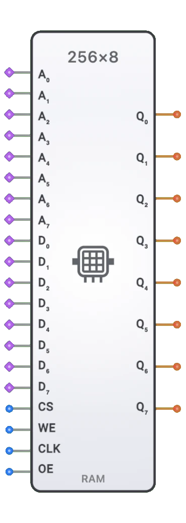
- Simbolo: La RAM esta representada por un bloque rectangular con entradas de direccion, entradas de datos y senales de control (CS, WE, CLK, OE), con salidas de datos a la derecha.
- Rol en DigiSim.io: Proporciona funcionalidad esencial de memoria para disenos de sistemas digitales, permitiendo el almacenamiento de datos, tablas de consulta y variables temporales en circuitos simulados.
Descripcion funcional
Comportamiento logico
La RAM almacena y recupera datos de direcciones de memoria especificadas. Su operacion esta controlada por entradas de direccion, lineas de datos y senales de control.
Modos de operacion:
- Operacion de lectura: Cuando CS=1, WE=0 y OE=1, los datos almacenados en la direccion especificada aparecen en los pines de salida (combinacional).
- Operacion de escritura: En un flanco ascendente de CLK cuando CS=1 y WE=1, los datos presentes en los pines de entrada de datos se almacenan en la direccion especificada (escritura sincrona/por reloj).
- Estado inactivo: Cuando CS=0, los pines de salida estan en estado de alta impedancia y no se realizan operaciones.
Tabla de verdad de senales de control:
| CS | WE | CLK | OE | Operacion |
|---|---|---|---|---|
| 0 | X | X | X | Inactivo (salidas alta-Z) |
| 1 | 0 | X | 0 | Salida inactiva (alta-Z) |
| 1 | 0 | X | 1 | Operacion de lectura (combinacional) |
| 1 | 1 | ↑ | X | Operacion de escritura (en flanco ascendente) |
Nota: X significa "no importa", ↑ indica flanco ascendente de reloj
Entradas y salidas
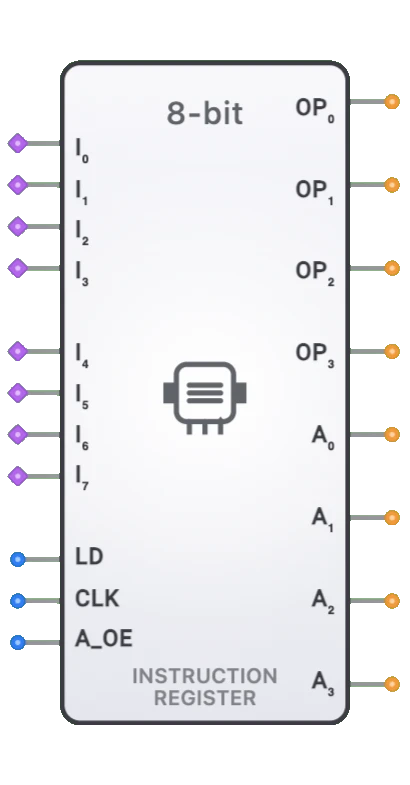
Entradas (20 en total):
- A0-A7: Pines 0-7. Entrada de direccion de 8 bits que especifica la ubicacion de memoria (hasta 256 ubicaciones).
- D0-D7: Pines 8-15. Entrada de datos de 8 bits (entradas de bus) para escritura de datos.
- CS (Chip Select): Pin 16. Activa la RAM cuando esta en HIGH.
- WE (Write Enable): Pin 17. Habilita la operacion de escritura cuando esta en HIGH (en conjunto con el flanco ascendente de CLK).
- CLK (Clock): Pin 18. Las operaciones de escritura ocurren en el flanco ascendente de CLK.
- OE (Output Enable): Pin 19. Habilita la salida de datos durante operaciones de lectura cuando esta en HIGH.
Salidas (8 en total):
- Q0-Q7: Salida de datos de 8 bits. Durante operaciones de lectura (CS=1, WE=0, OE=1), muestra el valor almacenado en la direccion especificada. De lo contrario, muestra alta impedancia (alta-Z).
Parametros configurables
- Tamano de memoria: La capacidad de la RAM en DigiSim.io, con un valor predeterminado de 256x8 (256 direcciones, 8 bits por direccion).
- Contenidos iniciales de memoria: Valores precargados opcionales para propositos de simulacion.
- Retardo de propagacion: El retardo de tiempo entre cambios de direccion/senal de control y la salida de datos.
Representacion visual en DigiSim.io
La RAM se muestra como un bloque rectangular con entradas y salidas claramente etiquetadas. Las entradas de direccion estan tipicamente en el lado izquierdo, con lineas de datos y senales de control dispuestas para mayor claridad. Cuando se conecta en un circuito, el componente indica visualmente las operaciones activas y el flujo de datos a traves de cambios de color en los cables de conexion. Algunas implementaciones pueden incluir una pantalla de contenidos de memoria con fines educativos.
Valor educativo
Conceptos clave
- Sistemas de memoria: Demuestra como las computadoras almacenan y recuperan datos.
- Decodificacion de direcciones: Ilustra la relacion entre direcciones binarias y ubicaciones de memoria especificas.
- Almacenamiento de datos: Muestra como se organiza la informacion binaria en la memoria de la computadora.
- Temporizado de lectura/escritura: Explica la coordinacion de senales de control para operaciones de memoria.
- Jerarquia de memoria: Introduce el concepto de diferentes tipos de memoria en sistemas informaticos.
Objetivos de aprendizaje
- Comprender los principios fundamentales de la memoria de acceso aleatorio.
- Aprender a realizar operaciones de lectura y escritura utilizando senales de control.
- Reconocer la importancia de la memoria en los sistemas de computacion digital.
- Aplicar componentes de RAM para construir soluciones de almacenamiento de datos en disenos digitales.
- Comprender la relacion entre direcciones de memoria y datos almacenados.
Ejemplos de uso/Escenarios
- Almacenamiento de datos: Almacenamiento de variables y resultados intermedios en sistemas digitales.
- Tablas de consulta: Implementacion de tablas de datos predefinidas para aproximacion de funciones o conversion de codigos.
- Memoria buffer: Creacion de almacenamiento temporal entre componentes de sistema digital con diferentes velocidades.
- Almacenamiento de programas: Cuando se precarga, almacenamiento de instrucciones para que un procesador las ejecute.
- E/S mapeada en memoria: Implementacion de perifericos direccionados por memoria en sistemas informaticos.
Notas tecnicas
- La RAM en DigiSim.io simula la naturaleza volatil de la RAM fisica, donde los datos se pierden cuando se retira la alimentacion o se reinicia la simulacion.
- Para una operacion correcta, las senales de control deben secuenciarse adecuadamente segun la tabla de verdad.
- El acceso a memoria requiere consideracion de parametros de temporizado incluyendo tiempo de configuracion de direccion y tiempo de retencion de datos.
- Cuando no esta seleccionada (CS=0) o cuando la salida esta deshabilitada (OE=0), las lineas de datos entran en estado de alta impedancia, permitiendo compartir el bus con otros dispositivos.
Detalle de implementacion de circuito
Estructura de celda de memoria
Celda SRAM (6T):
Estructura de celda SRAM de 6 transistores:
- T1, T2: Inversores acoplados cruzados formando un latch biestable
- T3, T4: Transistores de acceso controlados por la linea de palabra (WL)
- T5, T6: Transistores de pull-down
- Almacenamiento biestable: Los inversores acoplados cruzados mantienen el estado sin necesidad de refresco
- Lineas de bit (BL, BL̅): Deteccion diferencial para inmunidad al ruido
Celda DRAM (1T1C):
Estructura de celda DRAM de 1 transistor y 1 capacitor:
- T: Transistor de acceso controlado por la linea de palabra (WL)
- C: Capacitor de almacenamiento que retiene la carga representando un bit de datos
- Linea de bit (BL): Lee/escribe datos a traves del transistor de acceso
- Requiere refresco: La carga del capacitor se fuga, necesita ciclos de refresco periodicos
- Mayor densidad: La estructura mas simple permite mas memoria por area de chip
Decodificacion de direcciones
Los decodificadores de fila y columna convierten las entradas de direccion en senales de seleccion de fila y columna:
graph LR
    A03[Address A0-A3] --> RDEC[Row Decoder]
    A47[Address A4-A7] --> CDEC[Column Decoder]

    RDEC --> RS[Row Select 0-15]
    CDEC --> CS[Column Select 0-15]

    RS --> ARRAY[Memory Cell Array]
    CS --> ARRAY
Ruta de datos
graph LR
    subgraph Read Operation
        CELL1[Memory Cell] --> SA[Sense Amplifier]
        SA --> OBUF[Output Buffer]
        OBUF --> DOUT[Data Output]
    end

    subgraph Write Operation
        DIN[Data Input] --> IBUF[Input Buffer]
        IBUF --> WD[Write Driver]
        WD --> CELL2[Memory Cell]
    end
Componentes relacionados
- ROM (Memoria de solo lectura): Memoria no volatil que solo se puede leer
- PROM (ROM programable): Memoria programable una sola vez
- EPROM (PROM borrable): Borrable usando luz ultravioleta
- EEPROM/Memoria Flash: Memoria no volatil borrable electricamente
- Registro: Memoria pequena y rapida utilizada para almacenamiento temporal de datos
- Registro de desplazamiento: Memoria secuencial con capacidad de desplazamiento
- Controlador de memoria: Circuito que gestiona las operaciones de memoria
- Memoria cache: Memoria buffer de alta velocidad entre la CPU y la memoria principal
- Decodificador de direcciones: Convierte direcciones binarias en lineas de seleccion individuales
- Buffer FIFO/LIFO: Memoria de proposito especial con acceso primero en entrar-primero en salir o ultimo en entrar-primero en salir