The Unsung Hero: Why the NAND Gate is the Universal Building Block of Digital Logic

Why did the NAND gate — not the AND, not the OR, not even the NOR — become the king of commercial digital logic? The answer is not found in any truth table. It is found in the history of semiconductor manufacturing, in the economics of transistor physics, and in a series of engineering decisions made between the 1960s and 1990s that shaped the digital world we live in today.
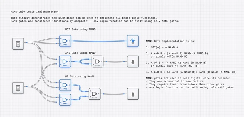
This post tells that story. For the mathematical proof of NAND universality, see our NAND to Tetris post. For NAND gate datasheets and CMOS implementation details, see our NAND in the real world post. This post is about why NAND won — the history, the trade-offs, and the engineering economics.
The NAND Gate: A Quick Refresher
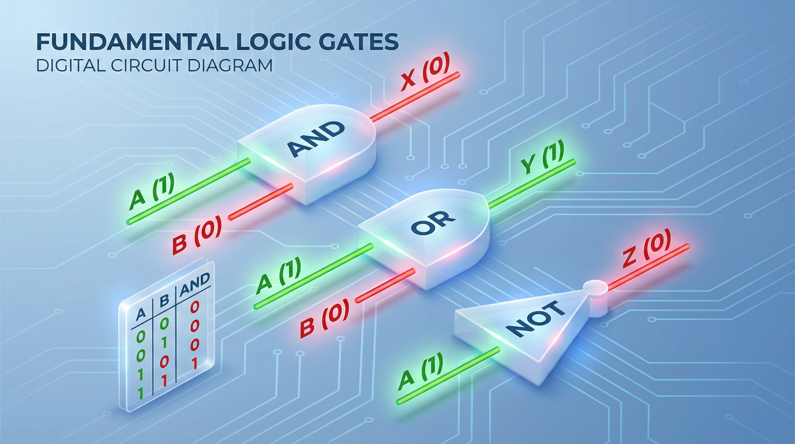
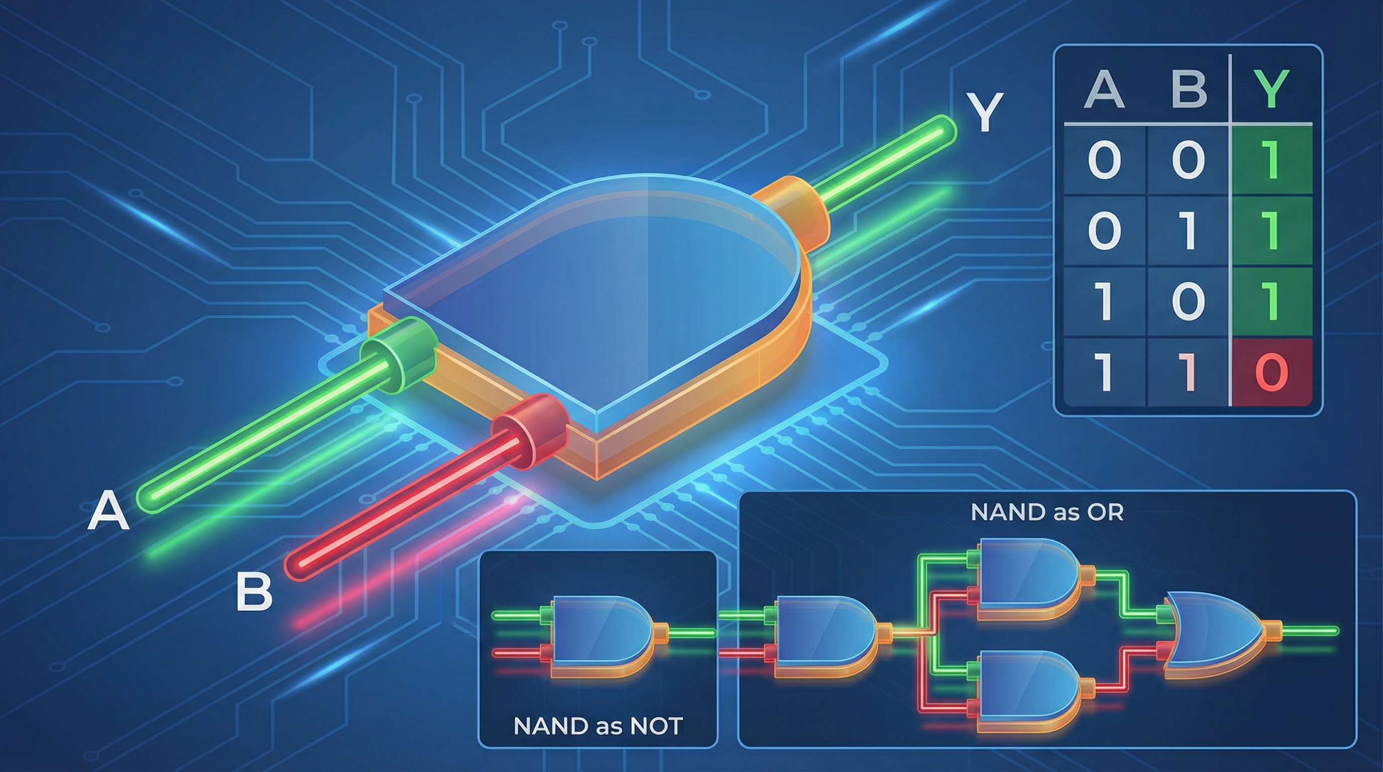
A NAND gate produces a LOW (0) output only when all of its inputs are HIGH (1). For every other input combination, the output remains HIGH (1).
| Input A | Input B | Output Y |
|---|---|---|
| 0 | 0 | 1 |
| 0 | 1 | 1 |
| 1 | 0 | 1 |
| 1 | 1 | 0 |
The Relay Era: Before Gates Had Names
Before there were transistors, there were relays. In the 1930s and 1940s, the earliest digital computers — machines like the Harvard Mark I and the Zuse Z3 — were built from thousands of electromechanical relays. Each relay was a switch controlled by an electromagnet: energize the coil, and the contacts close.
Engineers quickly realized that connecting relay contacts in series gave them AND logic (both must close), and connecting them in parallel gave them OR logic (either can close). Inversion was achieved using “normally closed” contacts that opened when energized.
These relay computers worked, but they were slow (milliseconds per operation), loud, and consumed enormous amounts of power. The logical functions were real, but the implementation was brutal. The dream of faster, smaller, quieter logic would require a fundamentally different kind of switch.
The Transistor Revolution: From Vacuum Tubes to Silicon
The invention of the transistor at Bell Labs in 1947 changed everything. Transistors could switch in microseconds rather than milliseconds, consumed far less power, and had no moving parts. By the late 1950s, engineers were building logic gates from discrete transistors on circuit boards.
But a critical question emerged: which logic family should dominate? In the early transistor era, multiple competing approaches existed:
- RTL (Resistor-Transistor Logic): Simple but slow and power-hungry.
- DTL (Diode-Transistor Logic): Better speed, but diodes degraded signal quality across cascaded stages.
- TTL (Transistor-Transistor Logic): Faster, with better noise margins and fan-out.
Each of these families had to choose a “native” gate — the gate that was simplest to implement in that technology. For TTL, that native gate was the NAND.
TTL and the Birth of the 7400 Series
In 1964, Texas Instruments introduced the SN7400 — a quad 2-input NAND gate IC in a 14-pin DIP package. It became one of the most successful integrated circuits in history, and the 7400 series it spawned defined digital design for decades.
Why was the NAND gate the foundation of TTL? Because of the “multi-emitter transistor” at the input stage. In TTL, the input transistor naturally produces an inverted AND function. Getting a non-inverted AND output required adding an extra transistor stage — additional cost, additional delay, additional power. The NAND was the path of least resistance.
The SN7400 sold for about $1 when introduced. By the 1970s, the price had dropped to pennies. Engineers designed entire computers — the PDP-11, early arcade machines, industrial controllers — primarily from 7400-series NAND gates and their derivatives (74LS, 74S, 74F for different speed/power trade-offs).
This was the period when NAND cemented its dominance. Not because of abstract mathematical universality, but because it was the cheapest, fastest, and most reliable gate you could buy.
The CMOS Transition: NAND’s Second Victory
In the 1980s and 1990s, the semiconductor industry shifted from TTL to CMOS (Complementary Metal-Oxide-Semiconductor) technology. CMOS offered dramatically lower power consumption — critical for the emerging laptop and mobile markets.
NAND won again in CMOS, but for different physical reasons than in TTL. In CMOS, a 2-input NAND gate uses two NMOS transistors in series (pull-down) and two PMOS transistors in parallel (pull-up). Because NMOS transistors have higher electron mobility (approximately 2-3x faster than PMOS), placing them in series is acceptable — the speed penalty is modest. The PMOS transistors in parallel present low resistance, yielding fast rise times.
The NOR gate has the opposite topology: PMOS in series, NMOS in parallel. Series PMOS transistors are slow and require larger sizing to match the NAND gate’s performance. This means a NOR gate consumes more area and more power for equivalent speed.
The result: CMOS standard cell libraries are NAND-dominated. A typical foundry library offers NAND2, NAND3, NAND4, and multiple drive-strength variants, all heavily optimized. NOR gates are available but used sparingly, typically only where the logic structure demands them.
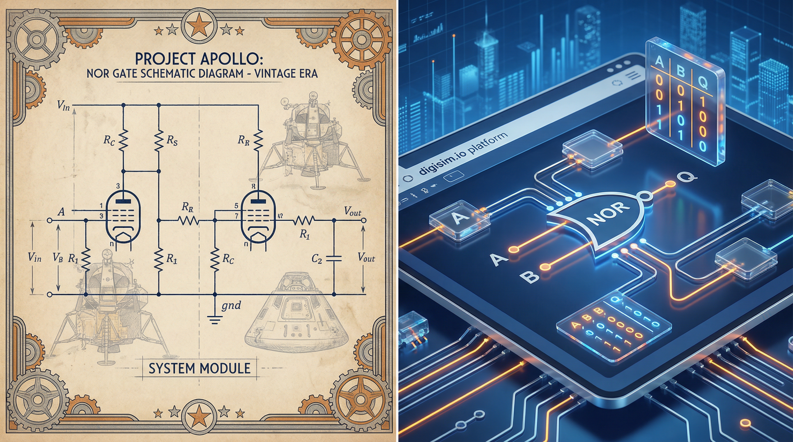
Why Not NOR? The Apollo Exception
The NOR gate is also functionally complete — it can build any logic function. And in one famous case, NOR was the chosen gate: the Apollo Guidance Computer (AGC), which used approximately 5,600 NOR gates to navigate astronauts to the Moon.
But the AGC was built with a different technology (Fairchild Micrologic RTL/DTL ICs) under different constraints. NASA’s primary concern was reliability, not density or speed. Using a single gate type simplified testing: if one NOR gate from a batch passed qualification, every gate in the batch was trusted.
In the commercial semiconductor market, where cost per transistor and clock speed determine market success, NAND’s physical advantages in both TTL and CMOS made it the winner. The Apollo Computer was an engineering triumph, but its design philosophy did not scale to mass-market consumer electronics.
For a detailed exploration of the NOR gate and the Apollo story, see our NOR gate post.
Engineering Economics: The Cost Argument
The economics of NAND dominance can be summarized in a few numbers:
| Metric | NAND2 (CMOS) | NOR2 (CMOS) | AND2 (CMOS) |
|---|---|---|---|
| Transistor count | 4 | 4 | 6 |
| Relative area | 1x | ~1.5x (due to PMOS sizing) | ~1.5x |
| Relative speed | 1x | ~0.6x-0.8x | ~0.8x (extra inverter stage) |
| Power (dynamic) | 1x | ~1.2x | ~1.2x |
When you multiply these differences by billions of gates on a modern SoC (System on Chip), the implications are enormous. A 10% area reduction can mean hundreds of millions of dollars in annual savings across a product line. A 20% speed improvement can define a new product generation.
This is why EDA (Electronic Design Automation) synthesis tools — the software that converts hardware description languages like Verilog and VHDL into physical gate layouts — are fundamentally NAND-biased. The technology mapping step preferentially decomposes Boolean functions into NAND-based implementations, only using other gate types when the logic structure specifically benefits from them.
NAND Flash: The Name Says It All
The most visible legacy of NAND gate economics is NAND Flash memory. In NAND Flash, floating-gate transistors are connected in series — the same series topology as the NMOS transistors in a CMOS NAND gate. This series connection makes each memory cell smaller than the parallel connection used in NOR Flash, enabling higher storage density.
When Toshiba’s Fujio Masuoka invented Flash memory in the 1980s, both NAND and NOR variants were developed. NOR Flash offered faster random read access (useful for code execution), but NAND Flash offered denser storage and faster writes. As the market shifted from code storage to data storage (music, photos, documents), NAND Flash won decisively. Today, NAND Flash is a multi-hundred-billion-dollar industry powering every SSD, smartphone, and USB drive on the planet.
Simulating the Historical Progression on digisim.io
You can trace this history yourself in digisim.io:
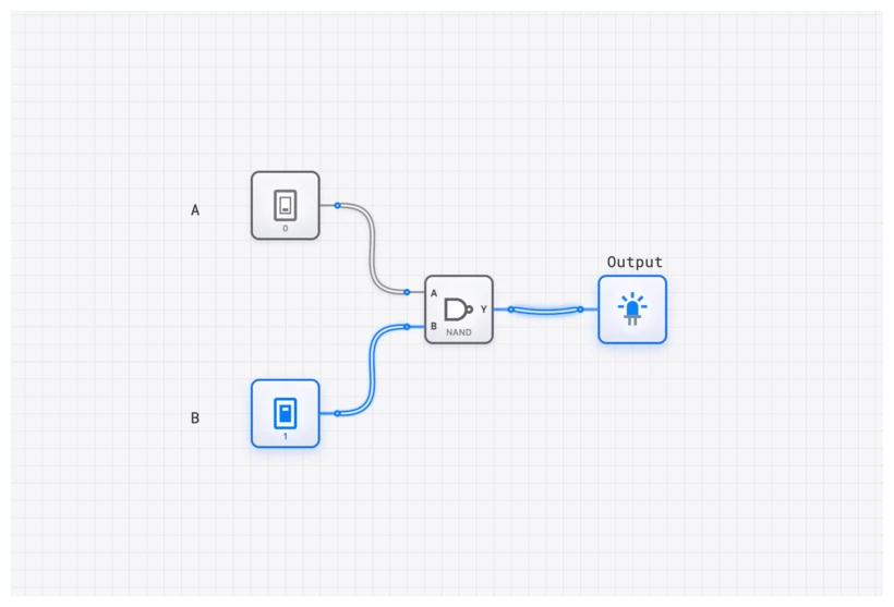
- Build a NAND-only NOT gate: Tie both NAND inputs together. This is how every TTL inverter was built internally.
- Build a NAND-only OR gate: Two NAND-as-inverter gates feeding into a third NAND. Count the gate levels (2) and measure the delay with the OSCILLOSCOPE.
- Build a NAND-only SR Latch: Cross-couple two NAND gates. This is the foundational memory cell — the same structure used in SRAM and register files inside every processor.
Each of these exercises recapitulates a step in the historical development of digital systems: from simple inversion, to combinational logic, to sequential memory.
Curriculum Connection
If you are following the structured learning path on digisim.io, this historical context enriches several modules:
- Universal Gates: Understanding why NAND is preferred, not just that it is universal.
- De Morgan’s Laws: The mathematical bridge between NAND and NOR representations.
- Memory Architecture: How NAND-based SR latches and D flip-flops form the basis of registers and SRAM.
Summary: The Engineering Perspective
The NAND gate did not become the foundation of digital logic because of a theorem. Functional completeness is shared with the NOR gate and, technically, with certain other gate combinations. NAND became dominant because of a convergence of physics, economics, and manufacturing reality:
- In TTL, the multi-emitter transistor naturally produced NAND.
- In CMOS, the NMOS-series/PMOS-parallel topology gave NAND the best speed-area-power trade-off.
- In Flash memory, the series transistor topology enabled denser storage.
- In EDA tools, NAND-biased synthesis produced smaller, faster chips.
Understanding this history transforms the NAND gate from an abstract symbol on a schematic into the product of decades of engineering optimization. It is the gate that won the silicon war — not by being the most elegant, but by being the most practical.