
The Unsung Hero: Why the Digital Buffer is Crucial for Complex Circuits
Discover why the seemingly inert digital buffer is actually a critical component for drive strength, signal integrity, and enabling complex architectures like shared buses.

In the world of digital logic, we are obsessed with transformation. We build circuits to add, subtract, compare, and manipulate data. An AND gate combines inputs, a NOT gate inverts them, and an XOR gate detects differences. Every gate seems to have a clear, transformative purpose. And then, we encounter the BUFFER—a gate whose output is logically identical to its input.
At first, this seems like an absurdity. Why dedicate precious silicon real estate to a component that, logically speaking, does nothing? This is the paradox of the buffer. Its value isn't in logical manipulation, but in physical restoration and control. It is the unsung hero that makes complex digital systems possible, solving real-world electrical problems that pure logic ignores. If you've ever wondered why your CPU doesn't just melt into a puddle of timing errors, you can thank the humble buffer.
The BUFFER: A Logical Identity
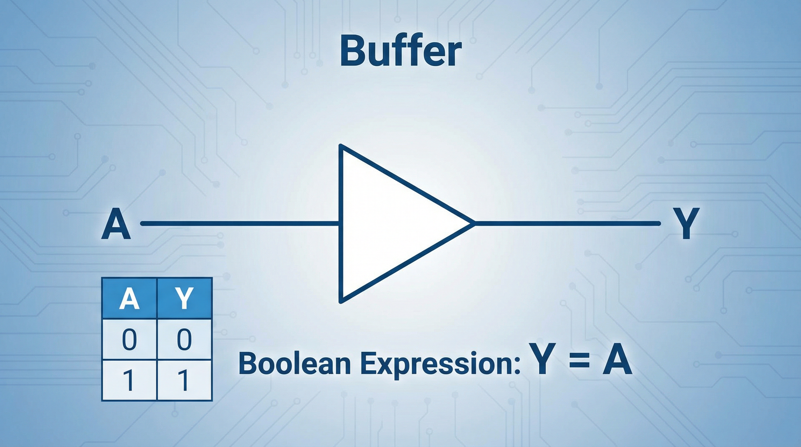
A BUFFER, or non-inverting buffer, is a single-input logic gate that produces an output identical to its input. If the input is HIGH (1), the output is HIGH (1). If the input is LOW (0), the output is LOW (0). It is the digital equivalent of a repeater, taking a signal and regenerating it.
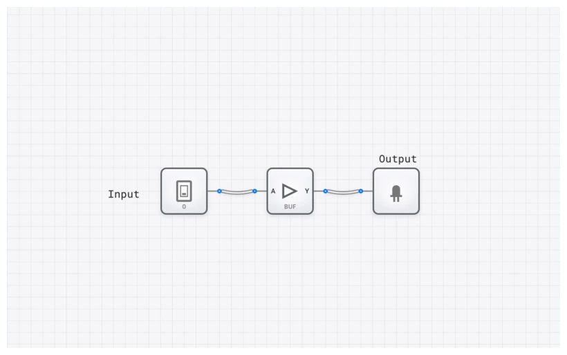
Its symbol is a simple triangle, representing the flow of signal from input to output without inversion. While it looks like a NOT gate without the bubble, its internal transistor structure is designed for a very different purpose: current gain.
Technical Specification: The Truth Table
The truth table for a BUFFER is the most straightforward in all of digital electronics, perfectly illustrating its function as a logical identity.
| Input (A) | Output (Y) |
|---|---|
| 0 | 0 |
| 1 | 1 |
Boolean Expression
The Boolean expression for a BUFFER is the essence of simplicity. For an input $A$ and an output $Y$, the equation is:
$Y = A$
This equation confirms that no logical operation is performed. The output simply equals the input. So, if the logic doesn't change, what does? To understand that, we have to step out of the world of "ideal" 1s and 0s and into the messy world of physics.
The "Gotcha": A BUFFER is Not Just a Wire
The most common mistake I see students make is equating a BUFFER with a simple wire. If both a wire and a buffer transfer a signal from point A to point B without changing its logical value, why bother with the component?
The difference lies in the physical domain. A wire is a passive conductor; it has resistance, capacitance, and inductance. A BUFFER is an active electronic component powered by a voltage source. This distinction is critical for two reasons: Drive Strength and Signal Integrity.
1. Drive Strength (Fan-Out)
A logic gate's output can only supply a finite amount of current. In digital design, we talk about "fan-out"—the number of subsequent gate inputs a single output can reliably drive. Imagine a single garden hose trying to fill ten swimming pools simultaneously. The pressure would drop to a trickle.
Similarly, if a gate's output is connected to too many inputs, its voltage level can "droop" into the undefined region (the "forbidden zone" between 0.8V and 2.0V in TTL logic). When this happens, the next gate in the chain might read a 1 as a 0, or worse, oscillate uncontrollably. A BUFFER acts like a pressure-booster pump. It takes a weak signal and provides a regenerated, high-current output capable of driving many subsequent loads.
2. Signal Integrity and Propagation Delay
As a signal travels down a long trace on a PCB or through a chain of logic gates, it degrades. Its sharp square edges become rounded and "mushy" due to parasitic capacitance. A BUFFER cleans this up, taking a distorted input and producing a crisp, clean, full-voltage output.
However, this "cleaning" isn't free. It takes time for the transistors inside the BUFFER to switch. This is known as propagation delay ($t_{pd}$).
$t_{pd} = t_{output} - t_{input}$
While we usually want to minimize delay, seasoned engineers actually use BUFFER components to add delay intentionally. If you have a race condition where a data signal is arriving slightly before a clock signal, dropping a few BUFFER gates in the path can slow the data down just enough to meet the setup time requirements of a D_FLIP_FLOP.
The Power of Three: The TRI_STATE_BUFFER
The standard BUFFER is powerful, but its sibling, the TRI_STATE_BUFFER, is what makes modern computer architecture possible. A TRI_STATE_BUFFER has two inputs: the data input ($A$) and an Enable ($E$) input.
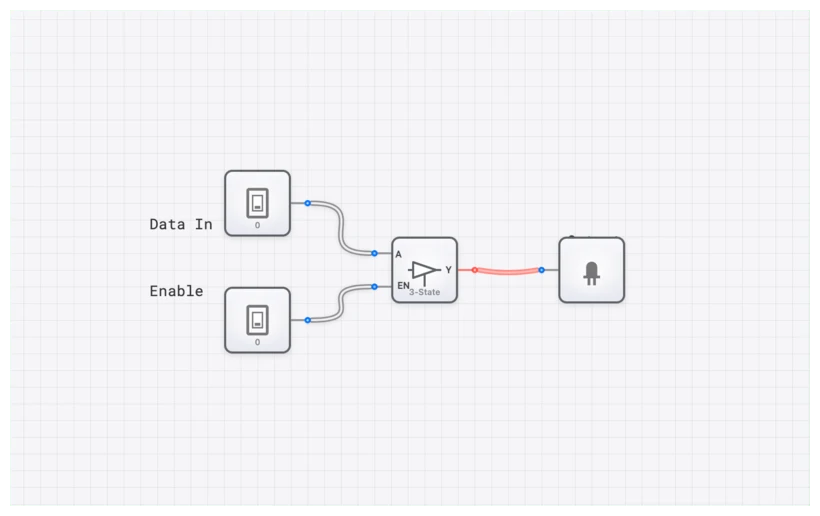
It can produce three output states:
- HIGH (1): When $E=1$ and $A=1$.
- LOW (0): When $E=1$ and $A=0$.
- High-Impedance (Z): When $E=0$.
The High-Impedance (or High-Z) state is the game-changer. In this state, the buffer's output is electrically disconnected from the circuit. It's not driving HIGH or LOW; it's effectively invisible. This allows multiple devices to share a common electrical pathway, or bus, without interfering with each other.
The Shared Bus Problem
Imagine two people trying to talk through a single megaphone at the same time. It would be gibberish. In electronics, if two gates try to drive the same wire—one driving HIGH and one driving LOW—you get "bus contention." This creates a short circuit, generates heat, and can destroy components.
By using TRI_STATE_BUFFER components, we ensure that only one device "owns" the bus at any given time. Everyone else stays in the High-Z state, "listening" but not "talking."
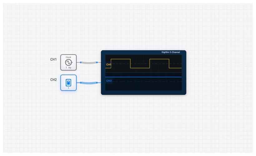
Verifying Behavior with the OSCILLOSCOPE
To truly appreciate what a BUFFER does, you need to see the timing. In digisim.io, we use the OSCILLOSCOPE to visualize signal propagation.
When you connect a CLOCK to a BUFFER and then to an OUTPUT_LIGHT, the light seems to blink perfectly in sync with the clock. But if you attach an OSCILLOSCOPE_8CH and zoom in on the nanosecond scale, you'll see the "aha!" moment. The output waveform of the BUFFER is shifted slightly to the right of the input waveform. That shift is the propagation delay $t_{pd}$.
In complex circuits, like an ADDER_8BIT, these delays accumulate. If you don't account for them, your ALU might produce the wrong result because the carry bit hasn't arrived yet. Using a BUFFER to align these signals is a fundamental skill in high-speed digital design.
Real-World Applications
1. Clock Distribution Networks (Clock Trees)
In a modern processor like an Intel Core i9 or an AMD Ryzen, there are billions of transistors that all need to flip at the exact same time. A single CLOCK source cannot possibly drive all those gates. Instead, engineers build "Clock Trees."
The master clock signal goes into a primary BUFFER, which drives four more buffers, which each drive sixteen more, and so on. This tree structure ensures that the clock signal has enough "muscle" (drive strength) to reach every corner of the chip simultaneously. Without buffers, the clock signal would be so weak by the time it reached the edge of the chip that the CPU would simply stop functioning.
2. Memory Interfacing (RAM)
Your computer's RAM is a perfect example of tri-state logic in action. Every memory chip in your system is connected to the same DATA_BUS_8BIT. When the CONTROL_UNIT wants to read from a specific memory address, it sends an "Enable" signal to the TRI_STATE_BUFFER of that specific chip. That chip then "talks" to the bus, while all other chips remain in High-Z. This is how 16GB of RAM can share the same 64 wires without a single collision.
Building it on digisim.io: A Practical Exercise
Let's put theory into practice. I want you to build a simple bus arbiter. This is the foundation of how a CONTROL_UNIT manages data flow.
- Setup the Inputs: Place two
INPUT_SWITCHcomponents. Label themData_AandData_B. - Add the Buffers: Place two
TRI_STATE_BUFFERcomponents. ConnectData_Ato the input of the first, andData_Bto the input of the second. - Create the Bus: Connect the outputs of both buffers together. This is your "Bus." Connect this bus to an
OUTPUT_LIGHTor aDIGIT_DISPLAY. - Control the Flow: Add two more
INPUT_SWITCHcomponents labeledEnable_AandEnable_B. Connect them to the enable pins of their respective buffers. - Test the Contention:
- Turn
Enable_AON andEnable_BOFF. ToggleData_A. The output followsData_A. - Turn
Enable_AOFF andEnable_BON. ToggleData_B. The output followsData_B. - The Danger Zone: Turn both
Enable_AandEnable_BON. SetData_Ato 1 andData_Bto 0. In digisim.io, you'll see the wire turn red. This is Bus Contention. You've just simulated a hardware conflict!
- Turn
Related Lessons in the Curriculum
If you're following our 70-lesson track, the BUFFER is a pivotal point where we move from "pure math" to "real engineering."
- Lesson 8: Basic Logic Gates (Introduction to the
BUFFERandNOTgates) - Lesson 31: Introduction to Multiplexers (How
TRI_STATE_BUFFERlogic compares to aMULTIPLEXER) - Lesson 63: Memory Architecture (Using buffers to build a functional
RAMsystem) - Lesson 68: CPU Bus Design (The final boss: managing the
DATA_BUS_8BIT)
Summary: The Unsung Hero
The next time you see a BUFFER in a circuit diagram, don't dismiss it as a "do-nothing" component. It is the gatekeeper of signal integrity. It provides the current to drive your displays, the timing to synchronize your ALU, and the isolation to allow your RAM to speak to your CPU.
In digital logic, as in life, sometimes the most important job isn't changing the message—it's making sure the message is strong enough to be heard.
Ready to master the bus? Head over to the editor and start building. I've set up a template for you to experiment with bus contention safely (without the smell of burning silicon).