Digital Buffers: Why They Matter in Complex Circuits
A buffer outputs its input unchanged — yet without it, clock trees and shared data buses cannot exist. Covers fan-out, tri-state, and bus contention.

TL;DR: A buffer outputs — logically a no-op — yet without it, complex digital systems cannot function. Buffers regenerate signal strength to satisfy fan-out limits, distribute clock signals through balanced trees, and (in the tri-state variant) let multiple drivers share a single bus by going to high impedance (Z) when not selected.
The buffer is logically a no-op: its output is identical to its input, . Yet a buffer is not a wire. Where a wire is a passive conductor with resistance and capacitance, a buffer is an active, powered component that regenerates signal strength. That distinction is what makes clock trees, fan-out, and shared data buses possible — solving electrical problems that pure logic ignores.
The BUFFER: A Logical Identity
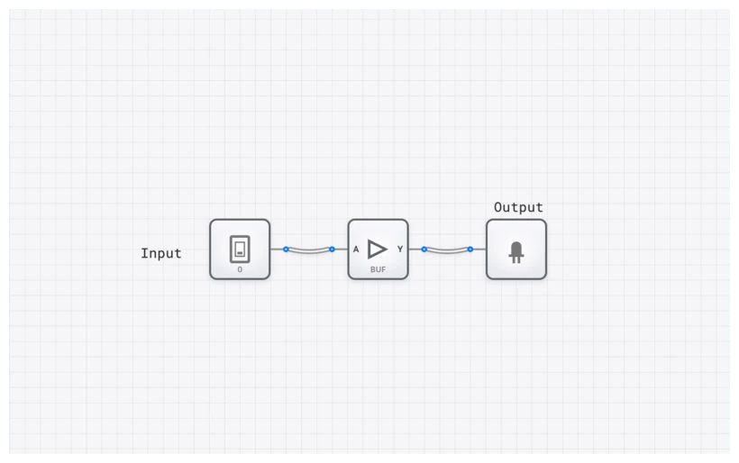
A BUFFER, or non-inverting buffer, is a single-input logic gate that produces an output identical to its input. If the input is HIGH (1), the output is HIGH (1). If the input is LOW (0), the output is LOW (0). It is the digital equivalent of a repeater, taking a signal and regenerating it to its full electrical potential.
In the hierarchy of digital systems, the BUFFER sits at the foundation of signal integrity. While it doesn’t change the “what” of the data, it fundamentally changes the “how”—specifically, how that data survives the journey across a circuit board or inside a microprocessor.
Technical Specification: The Identity Truth Table
The truth table for a BUFFER is the most straightforward in all of digital electronics, perfectly illustrating its function as a logical identity.
| Input (A) | Output (Y) |
|---|---|
| 0 | 0 |
| 1 | 1 |
Boolean Expression
The Boolean expression for a BUFFER is the essence of simplicity. For an input and an output , the equation is:
This equation confirms that no logical operation is performed. The output simply equals the input. But if the logic doesn’t change, what does? To understand that, we have to look past the 1s and 0s and look at the electrons.
Common Pitfall: A BUFFER is Not Just a Wire
The most common error — even from second-year computer engineering students — is equating a BUFFER with a simple wire. If both transfer a signal from A to B without changing its logical value, why not save the space and use copper?
The difference lies in the physical domain. A wire is a passive conductor; it has resistance, capacitance, and inductance. A BUFFER is an active electronic component powered by a voltage source. This distinction is critical for two reasons: Drive Strength and Timing.
1. Drive Strength and the Fan-Out Problem
Every logic gate has a limit to how much current it can “source” (push out from ) or “sink” (pull into ground). This limit defines its fan-out — the number of subsequent gate inputs it can reliably drive while maintaining valid logic levels.
Calculating Fan-Out
Fan-out is determined by the ratio of a gate’s output current capability to the input current required by each load gate:
The actual fan-out is the smaller of these two values. For example, a 74HC-series buffer might source 4 mA () and each 74HC input might require 1 uA (). Theoretically, this gives a fan-out of 4,000 — but in practice, capacitive loading limits the useful fan-out to around 10-20 gates at high frequencies, because each additional load gate adds input capacitance that slows down the signal transitions.
What Happens When Fan-Out is Exceeded
Imagine a single INPUT_SWITCH trying to trigger 50 AND gates. In a textbook, it works. In the real world, the voltage would droop. The signal would enter a “forbidden zone” — a voltage range that is neither a valid HIGH nor a valid LOW — leading to unpredictable behavior. Some gates might see a 1, others a 0, and some might oscillate.
A BUFFER solves this by acting as a current amplifier. It senses the weak input signal and uses its own power supply to regenerate a full-strength output. It “refreshes” the signal so it can drive those 50 gates reliably. In clock distribution networks, a single clock source drives a few buffers, each of which drives more buffers, creating a branching “clock tree” that can reach billions of transistors — see The Clock Pulse for the full distribution story.
2. Propagation Delay ()
Unlike an ideal wire in a textbook, a BUFFER takes time to work. This is known as propagation delay (). When the input flips from 0 to 1, the output doesn’t change instantly. There is a tiny, measurable lag—usually in the picoseconds or nanoseconds.
While we usually want circuits to be as fast as possible, designers often intentionally use BUFFER components to add delay. Why? To fix race conditions. If two signals need to arrive at a COMPARATOR at the exact same time, but one path is shorter than the other, you can add a chain of BUFFER gates to the faster path to “slow it down” and synchronize the system.
The Power of Three: The TRI_STATE_BUFFER
If the standard BUFFER is a signal refresher, its sibling, the TRI_STATE_BUFFER, is the traffic cop of the digital world. This component is what makes modern computer architecture—specifically the concept of a “bus”—possible.
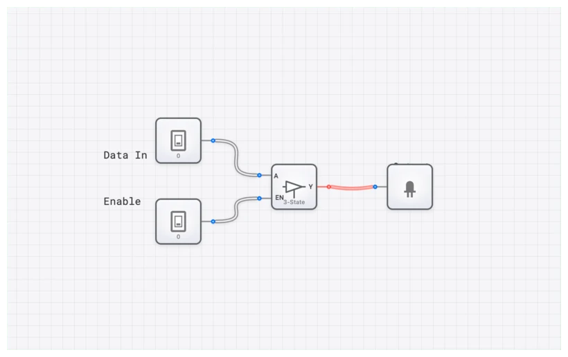
A TRI_STATE_BUFFER has two inputs: the data input () and an Enable () input. It can produce three distinct output states:
- HIGH (1): When is active and is HIGH.
- LOW (0): When is active and is LOW.
- High-Impedance (Z): When is inactive.
The High-Impedance (High-Z) state is the game-changer. In this state, the buffer’s output is electrically disconnected from the circuit. It’s not driving the line HIGH, and it’s not pulling it LOW. It’s effectively invisible.
Why High-Z Matters: Enabling Shared Data Buses
The High-Impedance state is what makes the concept of a “bus” possible in computer architecture. A bus is a set of shared wires that multiple devices can read from and write to — but not simultaneously.
Consider a simplified 8-bit CPU with four registers (R0-R3), an ALU, and a RAM module. All of these need to exchange data. Without tri-state buffers, you would need dedicated wires between every pair of components: R0-to-ALU, R1-to-ALU, R0-to-RAM, R1-to-RAM, and so on. For components, this requires connections — impractical for any non-trivial system.
With tri-state buffers, all components connect to a single shared data bus. Each component has a TRI_STATE_BUFFER on its output. At any given moment, exactly one component is “enabled” (its buffer is active), and all others are in High-Z. The enabled component drives the bus, and all other components can read from it.
| Enable (E) | Input (A) | Output (Y) |
|---|---|---|
| 0 | X (Don’t Care) | Z (High-Impedance) |
| 1 | 0 | 0 |
| 1 | 1 | 1 |
Bus Contention: The Danger of Multiple Drivers
What happens if two tri-state buffers driving the same bus are enabled simultaneously? If one tries to drive the line HIGH and the other tries to drive it LOW, you get bus contention — a short circuit between and ground through the two output transistors. This causes:
- Excessive current draw, potentially damaging the chips.
- An indeterminate voltage on the bus — neither a valid HIGH nor a valid LOW.
- Data corruption for any component trying to read the bus.
In digisim.io, bus contention is indicated by red wires, giving you immediate visual feedback. In real hardware, bus contention causes heat, wasted power, and unreliable operation. Preventing bus contention is a primary responsibility of the control unit, which must ensure that at most one device drives any bus at any time.
Active-Low vs. Active-High Enable
Many real-world tri-state buffers use an active-low enable pin (often written or ). This means the buffer is enabled when the control signal is LOW (0), and enters High-Z when the control signal is HIGH (1). Active-low enables are preferred in hardware because they can be driven directly by decoder outputs (which are typically active-low) and because the convention pairs naturally with a pull-up resistor on the enable line — if the driving signal disappears or is undriven at power-up, the pull-up holds the pin HIGH, disabling the buffer (the safe state). Note: an entirely floating CMOS input is indeterminate, not “HIGH” — it can drift, oscillate, and waste power. Always pull unused inputs to a known level.
Verifying Behavior with the OSCILLOSCOPE
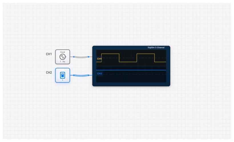
To truly appreciate the BUFFER, you need to see the timing. In digisim.io, we can use the OSCILLOSCOPE to visualize the relationship between input and output.
When you place a BUFFER and connect a CLOCK to its input, you can attach one channel of an OSCILLOSCOPE to the input and another to the output. In a real-world high-speed simulation, you would see the output waveform slightly shifted to the right of the input waveform. This shift represents the .
The Debugging Tip: If your complex CPU project on digisim.io is behaving erratically—perhaps a REGISTER is capturing the wrong data—check your timing. Use the OSCILLOSCOPE_8CH to look at the Enable signal of your TRI_STATE_BUFFER versus the data on the DATA_BUS_8BIT. If the buffer is disabled too early, the data will vanish into High-Z before the register can grab it.
Real-World Applications
1. Clock Distribution Networks (Clock Trees)
In a modern processor running at 3 GHz, the clock signal must reach billions of transistors within a fraction of a nanosecond. A single CLOCK source cannot possibly drive that many gates. Instead, engineers use a “Clock Tree” — a hierarchical structure of buffers.
The master clock drives a root buffer. That buffer drives 4-8 child buffers. Each child drives more buffers, and so on, creating a massive branching structure. The buffers at each level serve two purposes:
- Signal restoration: Each buffer regenerates a clean, full-swing square wave from a potentially degraded input.
- Skew minimization: By carefully balancing the path lengths through the tree, engineers ensure the clock arrives at all flip-flops within a tight timing window (typically under 100 ps of skew for modern processors).
The total buffer count in a clock tree for a modern SoC can exceed 100,000. Clock tree synthesis is one of the most critical steps in the physical design flow.
2. The Bidirectional Data Bus
RAM read and write operations occur over the same set of wires. This is achieved using pairs of TRI_STATE_BUFFER components facing in opposite directions:
- Write cycle: The CPU’s output buffers are enabled, driving data onto the bus. The RAM’s output buffers are in High-Z, and the RAM’s input latches capture the data.
- Read cycle: The CPU’s buffers go to High-Z. The RAM’s output buffers are enabled, driving stored data onto the bus for the CPU to read.
This “dance” happens millions of times per second and is orchestrated by the memory controller, which generates the enable signals in the correct sequence with precise timing.
3. Level Shifting and Voltage Translation
In modern systems, different subsystems often operate at different voltage levels. A 3.3V microcontroller might need to communicate with a 1.8V sensor and a 5V display driver. Specialized buffer ICs (like the TXB0108 or SN74LVC8T245) perform voltage translation while maintaining signal integrity. These are essentially buffers with different supply voltages on their input and output stages.
4. I/O Protection and ESD
Every I/O pin on a microcontroller or FPGA has buffer stages at the pad. These buffers protect the internal circuitry from electrostatic discharge (ESD) and provide the current drive needed to communicate with external devices. Without these buffer stages, the delicate internal logic transistors would be damaged by the harsh electrical environment of the outside world.
Hands-On: Building a Shared Bus on digisim.io
Let’s put theory into practice with two exercises: a basic shared bus and a more advanced 4-register data transfer system.
Exercise 1: Two-Source Shared Bus
This demonstrates the fundamental tri-state bus concept.
- Setup Inputs: Place two INPUT_SWITCH components. Label them
Data_AandData_B. - Add Control: Place two more INPUT_SWITCH components. Label them
Enable_AandEnable_B. - Place Buffers: Add two TRI_STATE_BUFFER components.
- Connections:
- Connect
Data_Ato the input of the first buffer. - Connect
Enable_Ato the enable pin of the first buffer. - Connect
Data_Bto the input of the second buffer. - Connect
Enable_Bto the enable pin of the second buffer.
- Connect
- The Bus: Connect the outputs of both buffers to a single OUTPUT_LIGHT.
- Simulation:
- Turn on
Enable_A. ToggleData_A. The light followsData_A. - Turn off
Enable_Aand turn onEnable_B. The light now followsData_B. - The Danger Zone: Turn on both
Enable_AandEnable_BwhileData_Ais 1 andData_Bis 0. In digisim.io, the wires turn red. This is Bus Contention — you have simulated a short circuit.
- Turn on
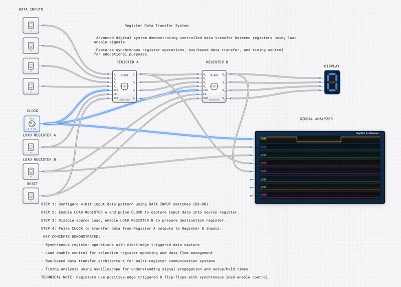
Exercise 2: Four-Register Data Transfer
This exercise models a simplified CPU data bus.
- Place four INPUT_SWITCH components labeled
R0_Data,R1_Data,R2_Data,R3_Data(representing register outputs). - Place four TRI_STATE_BUFFER components.
- Place four INPUT_SWITCH components for the enable lines:
R0_EN,R1_EN,R2_EN,R3_EN. - Connect each data switch to its corresponding buffer input, and each enable switch to its buffer enable.
- Connect all four buffer outputs to a single shared wire leading to an OUTPUT_LIGHT labeled “BUS”.
- Add an OSCILLOSCOPE: connect Channel 1 to R0’s buffer output, Channel 2 to R1’s buffer output, and Channel 3 to the BUS line.
Test protocol: Enable R0 and set its data to 1. Observe the BUS light ON. Disable R0 and enable R1 with data = 0. Observe the BUS light OFF. Practice the “break before make” discipline: always disable the current driver before enabling the next one. This prevents bus contention and is the same protocol used in real CPU bus controllers.
Related Topics in the Curriculum
- The Humble NOT Gate — buffer is to NOT what AND is to NAND.
- The SR Latch — feedback loops with cross-coupled gates.
- Mastering the 4-Bit Register — where tri-state buffers gate register output onto a shared bus.
- The Clock Pulse — buffer-based clock trees for skew minimization.
Summary: The Buffer in Context
The buffer is unique among logic gates because its value is entirely physical, not logical. It does not transform data; it transforms the electrical characteristics of a signal. Here is a summary of when to use each buffer variant:
| Situation | Solution |
|---|---|
| Signal too weak to drive multiple loads | Standard BUFFER (fan-out amplification) |
| Multiple sources sharing one wire | TRI_STATE_BUFFER (bus arbitration) |
| Need intentional delay on a signal path | BUFFER chain (delay insertion) |
| Different voltage domains communicating | Level-shifting buffer IC |
| Clock signal needs to reach many flip-flops | BUFFER tree (clock distribution) |
Final Thoughts
The BUFFER is glue, not logic. It provides physical drive strength, timing precision, and (in the tri-state variant) the ability to share resources via High-Z. When signals on a complex digisim.io circuit are not reaching their destination, the answer is often not more logic — it is a BUFFER.
For the next step, read Mastering the 4-Bit Register to see tri-state buffers gate register output onto a shared bus, then Open the BUFFER component reference to verify the truth table.