Setup, Hold, and Metastability in Digital Circuits
Setup and hold times define a forbidden window around each clock edge. Violations cause metastability — mitigated by 2-flip-flop synchronizers.

TL;DR: Every flip-flop has a setup time () before the clock edge and a hold time () after it during which the data input must remain stable. Violating these constraints can drive the flip-flop into a metastable state — an unresolved voltage between HIGH and LOW that resolves probabilistically. The standard mitigation is a two-stage synchronizer: two flip-flops in series, both clocked, that give the first stage a full clock period to settle.
Logically flawless CPU architectures fail the moment they meet real hardware or high-fidelity simulation if their authors ignored timing. The flip-flop is not the perfect, instantaneous device drawn in diagrams — it is a physical circuit with rules, and breaking them produces unpredictable behavior. This post unpacks setup time, hold time, and metastability, and shows the standard engineering response.
What Is a Setup-Time Violation?
In an introductory logic course, the D_FLIP_FLOP is treated as a perfect one-bit memory cell. On the rising edge of a CLOCK signal, it copies its D input to its Q output and holds it until the next clock edge. Clean, predictable, and in an ideal world instantaneous.
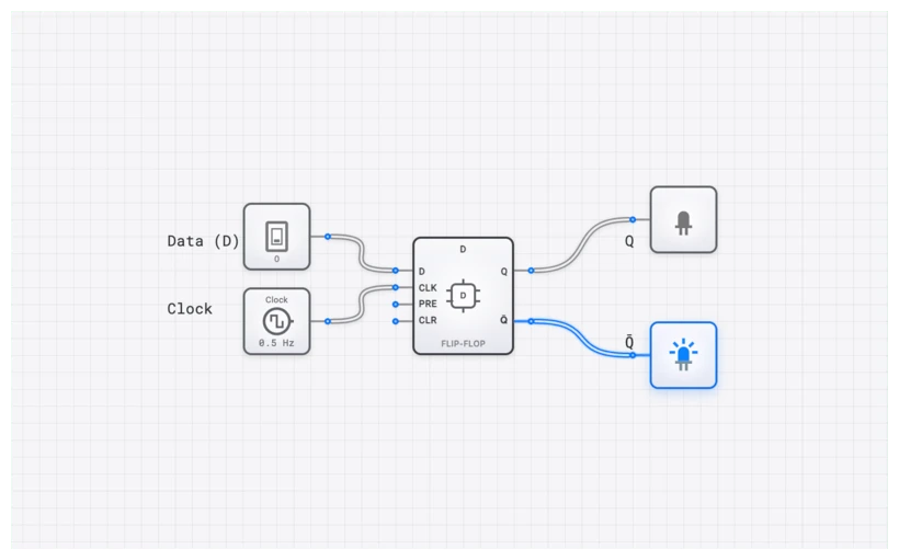
But reality is messy. A D_FLIP_FLOP is constructed from internal gates—usually a master-slave arrangement of latches. These gates are made of transistors that require a finite amount of time to switch states, charge internal capacitances, and reach a stable voltage. Because of this, the flip-flop cannot sample a moving target. For a clean data capture, the input signal must be stable for a brief period around the clock’s active edge.
If you try to change the input exactly when the clock strikes, you aren’t giving the internal feedback loops enough time to “decide” whether the new state is a 0 or a 1. This is where the “forbidden zone” comes into play.
The Technical Specification: D_FLIP_FLOP
Before we dive into the timing violations, let’s establish the baseline behavior. The D_FLIP_FLOP is an edge-triggered device. Unlike a D_LATCH, which is transparent while the enable signal is high, the flip-flop only “samples” the input at a specific transition (usually the rising edge).
Truth Table
| CLOCK | D | Description | |
|---|---|---|---|
| ↑ | 0 | 0 | Reset state captured on rising edge |
| ↑ | 1 | 1 | Set state captured on rising edge |
| 0/1/↓ | X | Q | No change; maintains previous state |
The Boolean characteristic equation for the D_FLIP_FLOP is deceptively simple:
However, this equation only holds true if we respect the timing constraints of the physical implementation.
The “Forbidden Zone”: Setup and Hold Time
Think of a flip-flop as a high-speed camera taking a picture on the clock’s flash. For a clear photo, your subject (the data) must be perfectly still just before, during, and just after the flash. If the subject moves while the shutter is open, the photo is a blur.
1. Setup Time ()
This is the minimum time the data input must be stable before the active clock edge arrives. It’s the “hold still!” warning before the camera flash. The flip-flop’s internal circuitry needs this time to propagate the D signal through the first stage of the master-slave latch. If the data changes during this window, the internal nodes may not reach the threshold voltage required to trigger a state change.
2. Hold Time ()
This is the minimum time the data input must remain stable after the active clock edge has passed. You can’t move the instant the flash is over; the camera’s shutter is still technically closing. The flip-flop needs this time to reliably “lock” the captured value into its feedback loop. If D changes too quickly after the clock edge, the new value might “leak” into the latch before it has fully closed, corrupting the stored bit.
Together, and create a forbidden zone around the clock edge. If a transition occurs on the D line within this window, the output of the flip-flop becomes unpredictable.
The Consequence of Violation: Metastability
So what happens if we break the rules? What if our data signal changes right inside that forbidden zone? The result is metastability.
Metastability is the digital equivalent of a coin landing perfectly on its edge. It is an unstable equilibrium. In a metastable state, the flip-flop’s output (Q) doesn’t cleanly snap to a 0 or a 1. Instead, it might:
- Hover at a voltage halfway between HIGH and LOW (the “invalid” logic zone).
- Oscillate rapidly between 0 and 1 as the internal feedback loop struggles to settle.
- Eventually, randomly, settle to either a 0 or a 1—but only after a significant delay.
This is catastrophic. A metastable signal propagating to other parts of your circuit can cause a cascade of failures. Imagine an ALU_8BIT receiving a metastable input; its internal ADDER components would produce garbage results. A PROGRAM_COUNTER_8BIT in a metastable state could cause the CPU to jump to a random, invalid memory address, leading to a hard system crash.
The Probability of Failure
The time it takes for a metastable state to resolve is probabilistic. While it usually resolves within a few nanoseconds, there is a statistically non-zero chance it could persist for a dangerously long time. We measure this reliability using the Mean Time Between Failures (MTBF):
In this formula:
- is the time allowed for the signal to resolve (usually the remainder of the clock cycle, ).
- is a flip-flop characteristic constant — the metastability resolution time constant, typically tens of picoseconds in modern processes.
- is the metastability window — the slice of the clock period during which an input transition can produce metastability. Also a flip-flop characteristic.
- is your system clock frequency.
- is the frequency at which your asynchronous input changes.
The takeaway is sobering. As you raise the clock frequency, shrinks (less of each clock period is left for resolution). MTBF is exponential in , so a small drop in produces an enormous drop in reliability. Doubling can collapse MTBF by orders of magnitude — not just halve it. This is why high-speed systems are so much more sensitive to timing issues than hobbyist projects running at 1 Hz.
The Engineer’s Solution: The Two-Stage Synchronizer
In the real world, you cannot avoid asynchronous signals. User inputs from an INPUT_SWITCH, data arriving from a different clock domain, or sensor readings are all “asynchronous”—they have no relationship to your system CLOCK. They will eventually violate a setup or hold time. It’s not a matter of if, but when.
So how do we safely bring these “wild” signals into our synchronous world? We use a Two-Stage Synchronizer.
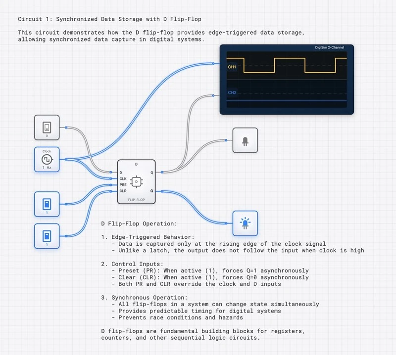
The design is elegantly simple: chain two D_FLIP_FLOP components together in series, both driven by the same system CLOCK.
- First Stage (FF1): The asynchronous input is fed into FF1. This is the “sacrificial” stage. We expect FF1 to go metastable occasionally—that is its job.
- Second Stage (FF2): The output of FF1 is fed into the D input of FF2. No combinational logic is placed between FF1 and FF2.
How it works: By the time the next clock edge arrives at FF2, the output of FF1 has had one full clock cycle () to resolve its metastability. For most modern digital systems, one clock cycle is an eternity compared to the metastability resolution time constant () of the flip-flop. The probability of FF1 still being metastable when FF2 samples it is exponentially small.
The MTBF of the two-stage synchronizer is:
For a well-designed synchronizer at 100 MHz with typical flip-flop parameters, the MTBF can exceed thousands of years.
Clock Domain Crossing
The two-stage synchronizer is the standard solution for clock domain crossing—the problem of passing data between two parts of a system that run on different, unrelated clocks. In modern SoCs (System on Chip), it is common to have dozens of independent clock domains (CPU core, memory controller, USB interface, display controller, etc.). Every signal that crosses from one domain to another must pass through a synchronizer, or the receiving domain risks metastable corruption.
For multi-bit data crossing clock domains, a simple two-stage synchronizer is insufficient (each bit might resolve to a different clock cycle, corrupting the multi-bit value). The standard solutions include:
- Gray code encoding for counters (only one bit changes at a time, so a single-bit synchronizer suffices).
- Asynchronous FIFOs with dual-port RAM and Gray-coded read/write pointers synchronized independently.
- Handshake protocols with request/acknowledge signals, each synchronized separately.
The two-stage synchronizer is the atomic building block from which all of these more complex crossing structures are built.
Propagation Delay: The Speed Limit of Logic
Even when we respect setup and hold times, we aren’t out of the woods. Once a D_FLIP_FLOP successfully captures data, it takes time for that data to actually appear at the Q output. This is the Propagation Delay (), often called the Clock-to-Q delay ().
This delay is the physical time required for the signal to ripple through the internal gates of the flip-flop. It is the fundamental “speed limit” of your hardware.
Calculating Maximum Clock Frequency ()
The timing parameters of your flip-flops, combined with the delay of your combinational logic, dictate the top speed of your system. Consider a path between two registers, Register A and Register B, with an ADDER_8BIT in between.
To ensure the system works, the total time for a signal to leave Register A, travel through the adder, and arrive at Register B must be less than one clock period ().
Where:
- is the propagation delay of the source flip-flop.
- is the worst-case delay through the combinational logic (the “critical path”).
- is the setup time of the destination flip-flop.
If you try to run your clock faster than this (), the data won’t reach Register B in time for the next clock edge. You’ll violate the setup time, and your CPU will start hallucinating data. This is why “overclocking” a PC eventually leads to the Blue Screen of Death—you’ve pushed the clock period below the physical limits of the logic gates.
Visualizing Timing with the OSCILLOSCOPE_8CH
Theory is one thing, but seeing a signal “miss” a clock edge is a transformative experience for a student. In digisim.io, we provide the OSCILLOSCOPE and OSCILLOSCOPE_8CH specifically to debug these timing relationships.
For complex systems like an 8-bit CPU, the SimCast feature records circuit behavior so it can be replayed at slow speed and the signal propagation watched directly.
How to Debug Timing in digisim.io:
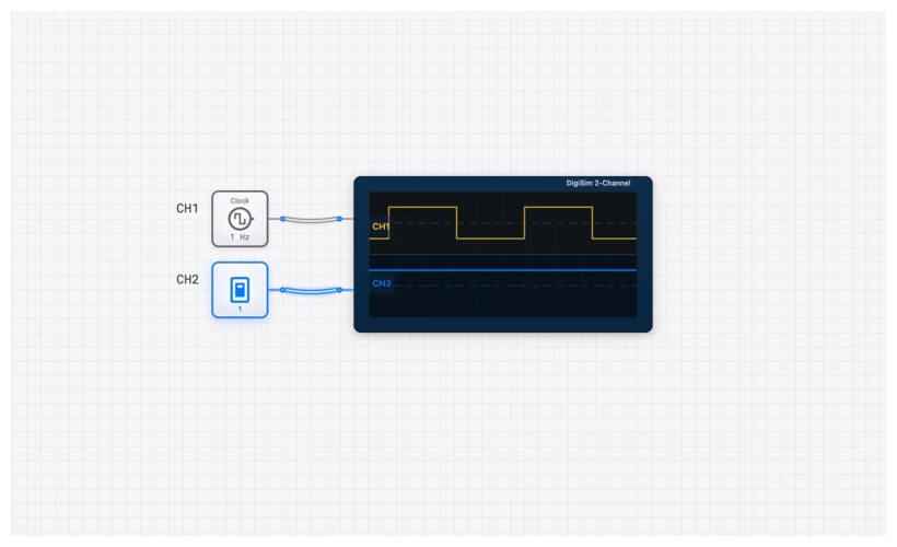
- Monitor the Clock: Connect Channel 1 of your OSCILLOSCOPE_8CH to your system CLOCK.
- Monitor the Data: Connect Channel 2 to the D input of a critical D_FLIP_FLOP.
- Monitor the Output: Connect Channel 3 to the Q output.
- Analyze the Gap: Look at the rising edge of the clock. Notice the tiny gap between the clock edge and the Q output changing? That’s your . Now, try to change your input right before the clock edge. If you see the output glitch or fail to update, you’ve just witnessed a setup time violation.
For a pre-configured setup, check out our D-Latch with Oscilloscope template. While a latch is level-sensitive, it’s the perfect playground for seeing how input changes interact with enable signals in real-time.
Visualize Timing with an Oscilloscope
Real-World Applications: From the 8086 to Modern FPGAs
These principles aren’t just academic. In the early days of computing, like with the Intel 8086, designers had to manually calculate these delays for every single trace on a circuit board. If one wire was slightly too long, the signal would arrive late, violating and breaking the processor.
In modern FPGA and ASIC design, we use “Static Timing Analysis” (STA) tools to do this for us. The tool looks at every path in the chip and ensures that is always less than the clock period. If it’s not, the tool “fails timing,” and the chip won’t be manufactured until the logic is redesigned or the clock speed is lowered.
Related Topics in the Curriculum
- The SR Latch — the basics of bistable memory.
- The D Flip-Flop — edge-triggered storage and master-slave construction.
- Propagation Delay — the physics of and critical paths.
- The Clock Pulse — frequency, duty cycle, skew, and jitter.
The Bottom Line for Reliable Design
The clock is a law of physics, not a suggestion:
- Respect the Window: Data must be stable before () and after () the clock edge.
- Fear Metastability: It is a probabilistic failure mode that resists simple debugging.
- Always Synchronize: Any signal from an INPUT_SWITCH or external source must pass through a two-stage synchronizer. No exceptions.
- Delay is the Limit: Maximum clock speed is dictated by the slowest logic path.
For the next step, see Mastering the 4-bit Register and put a synchronizer in front of every external input. Open the D_FLIP_FLOP component reference to start building.