Think about every interaction you have with a computer. You type a letter, and it stays on screen. You save a file, and it persists. You press a button in a game, and your character jumps. All of these depend on one fundamental capability: a circuit’s ability to remember.
But what does it mean for a circuit to remember? An AND gate does not remember. An OR gate does not remember. Feed them inputs and they produce an output. Remove the inputs and the output vanishes. They live entirely in the present, with no concept of “before.” So how do we cross the chasm from calculating to remembering? The answer is the SR Latch—and understanding it is one of the most important “aha moments” in all of digital design.
What Does It Mean to “Remember”?
Before we look at any circuit diagram, let’s think about what memory actually requires. Consider a hallway with two light switches at either end—a classic three-way switch arrangement. You flip one switch, and the light turns on. You walk away. The light stays on. Nobody is holding the switch. Nobody is providing continuous input. The physical arrangement of the circuit holds the state.
This is the key insight: memory is not a special material. It is a structural property. You do not need a special “memory chip” to store a bit. You need a feedback loop—a way for a circuit’s output to reinforce itself.
Imagine two friends standing in a room. Alice says, “I’ll stay quiet as long as Bob is talking.” Bob says, “I’ll stay quiet as long as Alice is talking.” Once Alice starts talking, Bob goes silent. Alice hears silence from Bob, which reinforces her decision to keep talking. The system is stable. It remembers who spoke first, even though nobody is forcing the issue anymore.
That is exactly how the SR Latch works.
The SR Latch: Two Gates That Remember
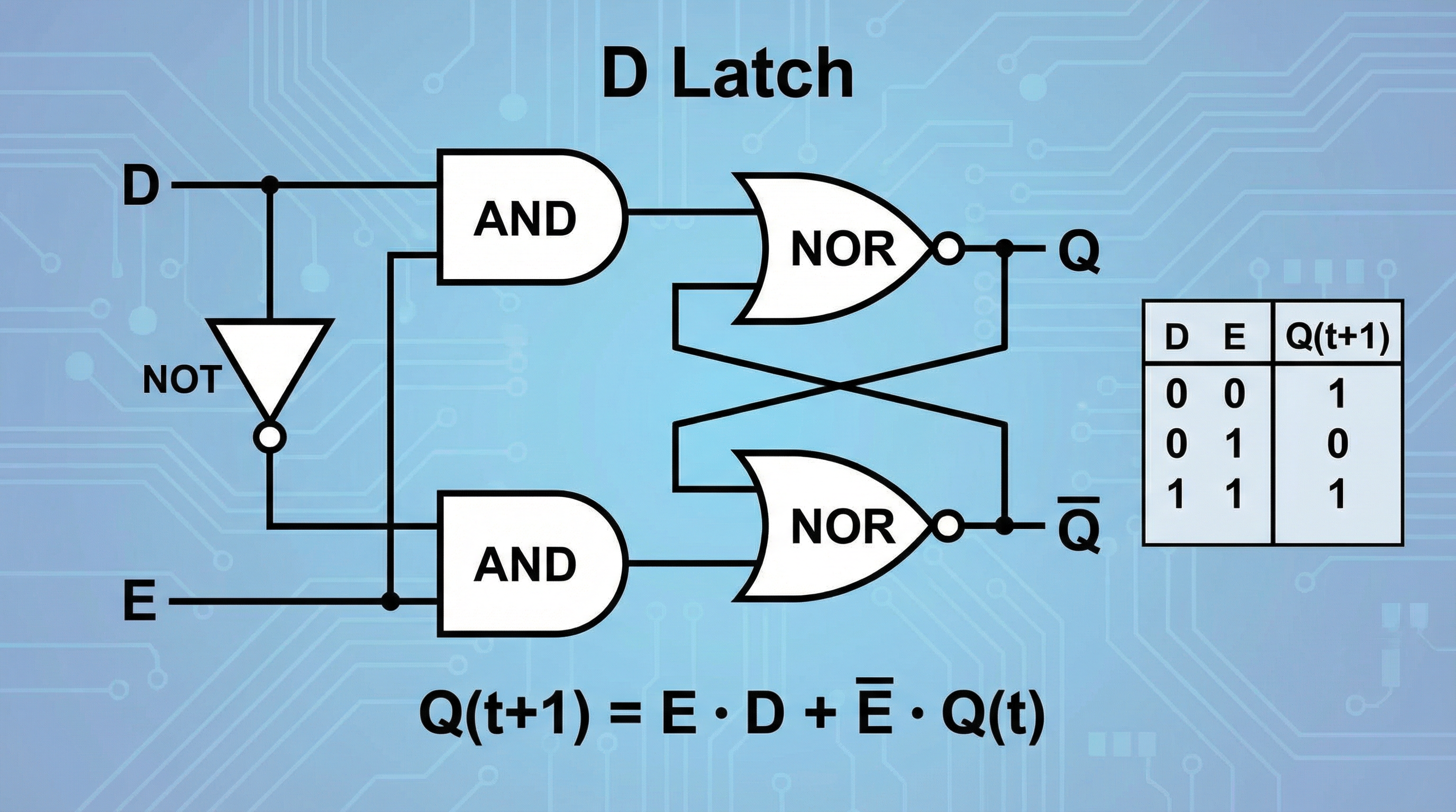
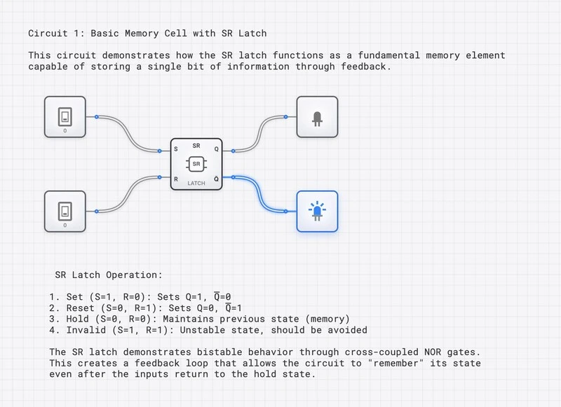
The SR Latch (Set-Reset Latch) is built from just two NOR gates wired in a feedback loop. The output of each gate connects to an input of the other. This cross-coupling creates a circuit with two stable resting states—what engineers call a bistable circuit.
The latch has two inputs and two outputs:
- S (Set): A brief pulse here stores a ‘1’.
- R (Reset): A brief pulse here stores a ‘0’.
- Q: The stored value.
- : The complement of Q (always the opposite).
Here is the truth table:
| S | R | Action | ||
|---|---|---|---|---|
| 0 | 0 | Q | Hold (Memory) | |
| 0 | 1 | 0 | 1 | Reset |
| 1 | 0 | 1 | 0 | Set |
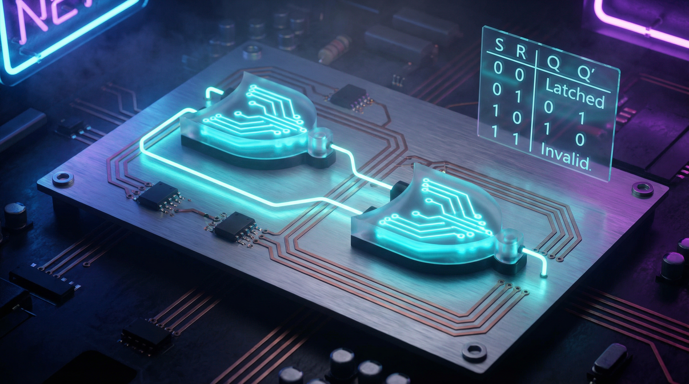
| 1 | 1 | 0 | 0 | Invalid (Forbidden) |
The most remarkable row is the first one: S=0, R=0. Both inputs are inactive, yet the output does not go to zero or become undefined. It holds whatever value it had before. The circuit remembers. No ongoing input is required to maintain the state.
The “Aha” Moment: Tracing the Feedback Loop
Let’s walk through what actually happens inside the circuit, step by step.
Setting the latch (storing a ‘1’):
- You pulse S to ‘1’. The bottom NOR gate sees a ‘1’ on its input and is forced to output ‘0’ (since any ‘1’ input to a NOR gate produces ‘0’).
- That ‘0’ travels up to the top NOR gate. The top gate now has both inputs at ‘0’, so it outputs ‘1’. This is our Q output—the stored bit.
- That ‘1’ from Q feeds back down to the bottom gate, reinforcing its ‘0’ output.
- Now remove the S pulse (set S back to ‘0’). The bottom gate still has a ‘1’ coming from Q on its other input, so it stays at ‘0’. The top gate still has both inputs at ‘0’, so it stays at ‘1’.
The feedback loop sustains itself. The latch has “remembered” the Set command, even though you removed the input. This is the moment where a combinational circuit becomes something more.
Resetting the latch (storing a ‘0’): The same process works in reverse through the R input, forcing Q to ‘0’ and to ‘1’.
The Forbidden State: What Goes Wrong
There is one input combination the SR Latch cannot handle: S=1 and R=1 simultaneously. You are telling the circuit to store a ‘1’ and a ‘0’ at the same time—a contradiction. Both gates are forced to output ‘0’, meaning Q and are both ‘0’. Since these are supposed to be complements of each other, the circuit is in a logically invalid state.
The real danger comes when both inputs return to ‘0’ simultaneously. Both gates race to output ‘1’, and the winner is determined by whichever gate happens to be a fraction of a nanosecond faster—something that depends on manufacturing tolerances, temperature, and even cosmic ray interference in extreme cases. The result is unpredictable. This limitation is important to understand, because solving it is what motivated the invention of the D Latch.
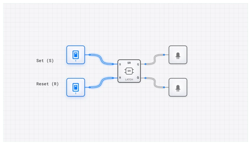
Try It: Build and Feel the Feedback
Reading about feedback loops and seeing one in action are two very different experiences. The best way to internalize this concept is to build the circuit yourself.
Step-by-Step Experiment:
- Initialize: Open the circuit. Both S and R should be ‘0’. The outputs might be in an arbitrary state.
- Set: Toggle the S switch to ‘1’. Watch Q light up.
- The Memory Test: Toggle S back to ‘0’. The Q light stays on. You just stored a bit of information using nothing but two logic gates. Let that sink in.
- Reset: Toggle the R switch to ‘1’. Q turns off, turns on.
- Hold Again: Toggle R back to ‘0’. The Reset state holds.
- The Forbidden Test: Toggle both S and R to ‘1’. Observe both outputs drop to ‘0’. Now toggle both back to ‘0’ and see which state the circuit settles into—it may surprise you.
Why Does This Matter? From Two Gates to Gigabytes
You might wonder: if this circuit is so simple, why is it important? Because the SR Latch is the ancestor of virtually every memory circuit in every digital device.
The Path from SR Latch to Your Computer’s RAM
The journey from this humble two-gate circuit to the gigabytes of memory in your computer follows a clear evolutionary path:
- SR Latch — Two cross-coupled gates that can hold one bit. (This is where you are now.)
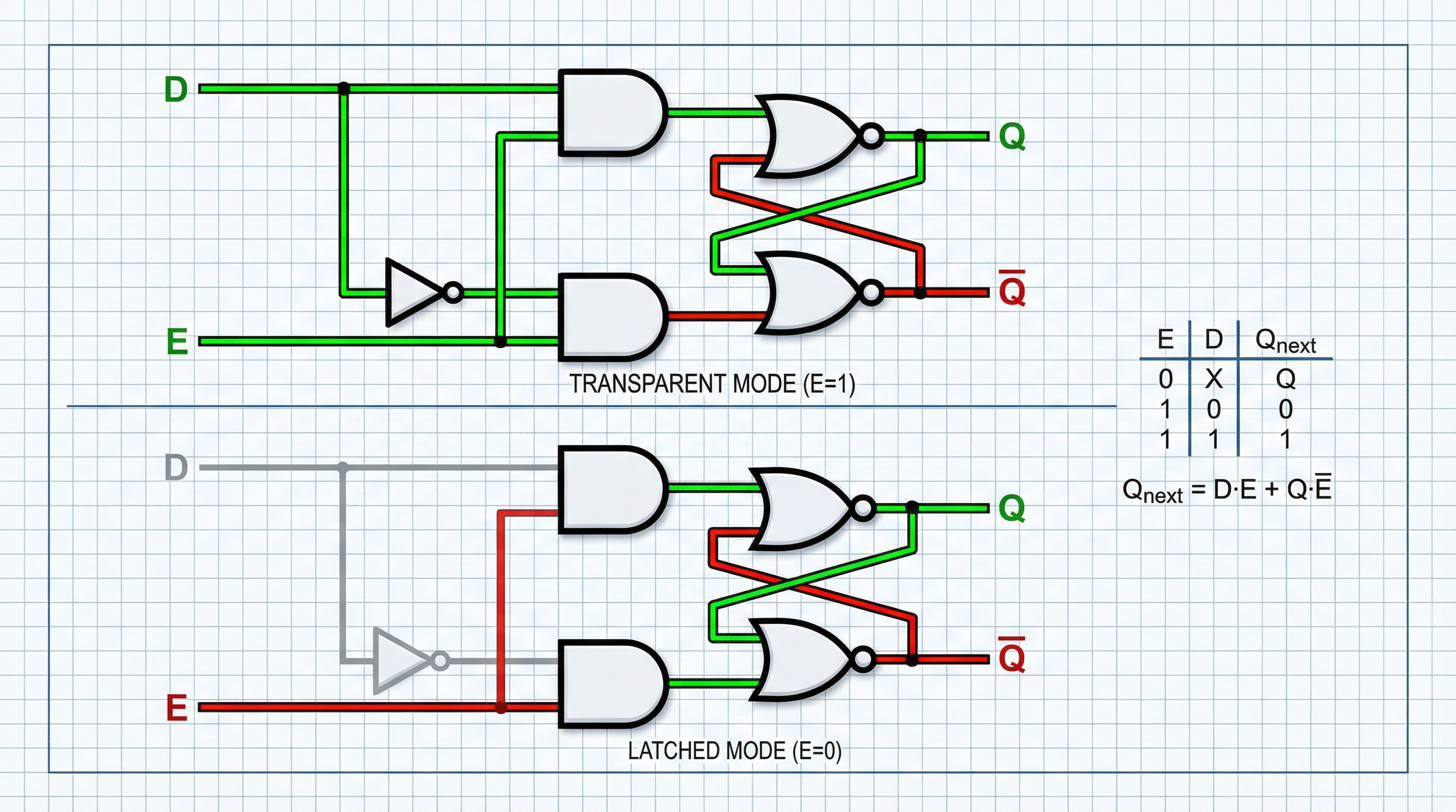
- D Latch — An SR Latch with added gating logic that eliminates the forbidden state and adds an Enable signal for controlled data capture.
- D Flip-Flop — A pair of D Latches arranged so data is captured only at the precise instant of a clock edge, enabling synchronized operation across millions of components.
- Register — A group of flip-flops (typically 8, 16, 32, or 64) that store a multi-bit value. CPU registers like the accumulator, program counter, and instruction register are all built from these.
- SRAM — Static RAM, the ultra-fast cache memory inside your CPU, uses a six-transistor cross-coupled structure that is a direct descendant of the SR Latch concept. Billions of these cells work in concert to give your processor instant access to frequently used data.
Every step in this chain builds on the feedback principle you just learned. The cross-coupled gate pair is the seed from which all digital memory grows.
Switch Debouncing: A Practical Application
The SR Latch also solves a real engineering problem. When you press a physical button, the metal contacts bounce for several milliseconds, generating a noisy burst of on-off signals. An SR Latch connected to a double-throw switch captures the first contact and ignores all subsequent bounces, producing a single clean pulse. This is how keyboards, arcade buttons, and industrial controls produce reliable signals from imperfect mechanical switches.
Related Topics
As you continue exploring digital logic on digisim.io, these topics build directly on what you have learned here:
- The SR Latch (Comprehensive) — A deeper technical treatment covering both NOR and NAND implementations, Boolean equations, and timing analysis.
- The D Latch — How engineers solved the forbidden state problem with a single inverter.
- Edge-Triggered Flip-Flops — Moving from level-sensitive latches to clock-synchronized memory, the basis of all modern synchronous logic.
Your Next Step
You have crossed a fundamental threshold. You now understand that memory is not a mysterious property of special hardware—it is the natural consequence of a feedback loop. Two gates, wired to reinforce each other, can hold a state indefinitely. From this simple idea, all digital memory follows.
Open the simulator, build the circuit, and experiment. Try setting and resetting. Watch the outputs hold their state with no ongoing input. Once you truly feel the feedback loop in action, you will never look at a computer the same way again.