The OR Gate: Understanding Digital Logic's Democratic Heartbeat
The OR gate outputs 1 if any input is 1. Truth table, Boolean expression, propagation timing, and uses in CPU interrupts, safety systems, and bus arbitration.

TL;DR: An OR gate produces a HIGH output when any one (or more) of its inputs is HIGH. Boolean expression . Where the AND gate demands unanimous consent, OR follows “any is enough” — the principle behind interrupt aggregation, alarm systems, and bus-request logic.
The OR gate is the democratic counterpart to the AND gate: it produces a HIGH output if even one input is HIGH. That “any is enough” rule makes it the natural primitive for interrupt aggregation, multi-sensor alarms, and bus arbitration — anywhere multiple independent sources need a single shared signal line.
Defining the OR Gate: The Logic of Disjunction
At its core, an OR gate is a digital logic device that implements logical disjunction. In plain English, it produces a HIGH output (logic 1) if one or more of its inputs are HIGH. The only way to get a LOW output (logic 0) is for every single one of its inputs to be LOW.
Think of it like a simple electrical circuit with two parallel switches controlling a light bulb. If you close Switch A, the light turns on. If you close Switch B, the light turns on. If you close both, the light is, of course, still on. The only way the bulb remains off is if both switches are open. The OR gate is the digital embodiment of this “either/or” logic. In the hierarchy of digital systems, the OR gate sits at the very foundation, right alongside the AND and NOT gates. Together, they form a functionally complete set, meaning you can build any possible digital system using just these three types of gates.
Technical Specification: The Truth Table
The behavior of any logic gate is formally defined by its truth table. This table exhaustively lists every possible combination of inputs and shows the resulting output. For a standard 2-input OR gate, the truth table is beautifully straightforward.
| Input A | Input B | Output Y |
|---|---|---|
| 0 | 0 | 0 |
| 0 | 1 | 1 |
| 1 | 0 | 1 |
| 1 | 1 | 1 |
The key takeaway is immediate: a single 1 on any input is sufficient to force the output to 1. This is the “inclusive OR” because it includes the case where both inputs are true. This is distinct from the XOR (Exclusive OR), where the output is HIGH only if the inputs differ.
The Language of Logic: Boolean Algebra
In the 19th century, George Boole developed an algebraic system to process logic, which now forms the mathematical foundation of all digital systems. In Boolean algebra, the OR operation is represented by a plus sign ().
For a 2-input OR gate with inputs and and output , the expression is:
It is absolutely critical to remember that this is logical OR, not arithmetic addition. In this context, . Why? Because the statement “true OR true” is simply “true.” This is a frequent point of confusion for beginners who are used to standard decimal math. Once you internalize that the symbol represents the union of possibilities rather than a sum of quantities, the elegance of Boolean notation becomes clear.
If we were to expand this to a 4-input OR gate, the expression would naturally follow:
In this scenario, if any variable ( or ) is 1, becomes 1.
Common Pitfall: Propagation Delay and Real-World Physics
In an ideal world—the kind we often draw on whiteboards—the moment an input to a logic gate changes, the output changes instantaneously. We, however, live in a world governed by the laws of physics. Transistors, the tiny switches that make up an OR gate, take a finite amount of time to move electrons and switch states. This inherent latency is known as propagation delay ().
For an OR gate, we specifically look at two metrics:
- : The time it takes for the output to transition from LOW to HIGH.
- : The time it takes for the output to transition from HIGH to LOW.
Why does this matter? Imagine you’re designing a CPU running at 3 GHz. At that speed, a single clock cycle is roughly 0.33 nanoseconds. If your OR gate has a propagation delay of 1 nanosecond, your signal won’t even finish moving through the gate before the next clock cycle starts.
This leads to “glitches” or “race conditions.” If two signals are supposed to arrive at an OR gate at the same time, but one travels through a longer path of wires, the gate might momentarily output a 0 when it should have stayed at 1. In high-speed digital design, we don’t just care about the logic; we care about the timing.
Verifying Behavior with the OSCILLOSCOPE
To truly understand propagation delay, you shouldn’t just take my word for it. You should see it. In digisim.io, we provide an OSCILLOSCOPE component that allows you to visualize these signals in real-time.
When you connect the inputs of an OR gate to one channel and the output to another, you’ll notice a tiny horizontal gap between the input rising and the output rising. That gap is your propagation delay. In a complex circuit, these delays add up (accumulate). If you chain ten OR gates together, the total delay is the sum of each individual gate’s . This is why “shallow” logic trees are preferred over “deep” ones in professional chip design.
Building the OR Gate in digisim.io
Theory is the map, but simulation is the journey. Let’s build a functional test-bench for an OR gate on the digisim.io canvas. This exercise will solidify your understanding of how signals propagate.
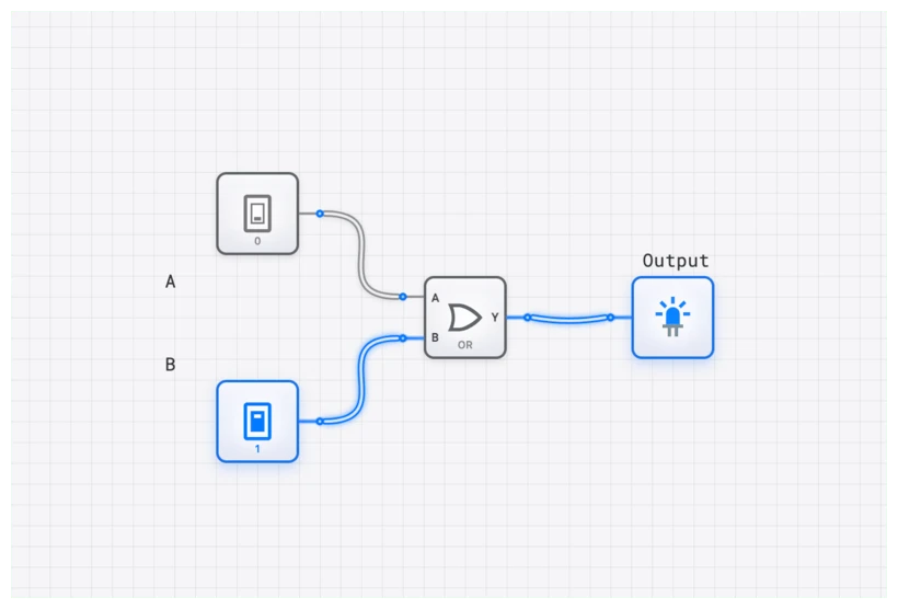
- Select Your Components: Open the editor and drag two
INPUT_SWITCHcomponents onto the canvas. Label them “A” and “B”. - Add the Gate: Grab the
ORgate from the Basic Logic Gates category. - Add Output: Drag an
OUTPUT_LIGHTto the right of the gate. - Wiring: Click the output pin of Switch A and drag it to the first input of the OR gate. Do the same for Switch B and the second input. Finally, connect the OR gate’s output to the
OUTPUT_LIGHT. - Test the Logic: Toggle the switches. You’ll see that the light only turns off when both switches are in the down (0) position.
If you want to get fancy, replace one INPUT_SWITCH with a CLOCK component. Now, the input will toggle automatically. Add an OSCILLOSCOPE and connect Channel 1 to the CLOCK and Channel 2 to the OR gate output. You’ll see the output perfectly mirroring the clock’s pulses—provided the other input is held at 0.
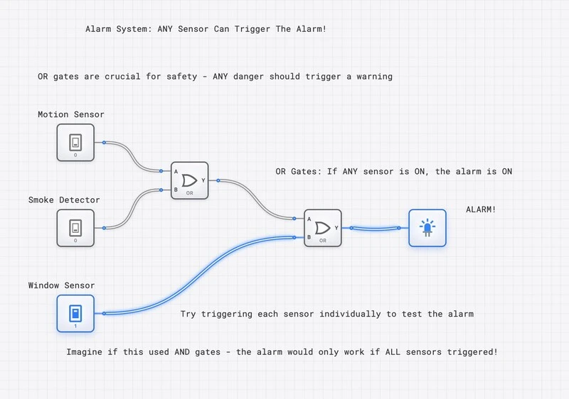
Detailed Build: A Multi-Sensor Alarm on digisim.io
Let’s extend the basic test circuit into a practical alarm system that demonstrates how OR gates aggregate multiple sensor inputs.
- Place Four INPUT_SWITCH Components: Label them “Door_Sensor”, “Window_Sensor”, “Motion_Detector”, and “Glass_Break”.
- Build a 4-Input OR Tree: Since digisim.io provides 2-input OR gates, cascade them. Feed Door_Sensor and Window_Sensor into the first OR gate. Feed Motion_Detector and Glass_Break into a second OR gate. Then feed the outputs of both gates into a third OR gate.
- Add Output: Connect the final OR output to an OUTPUT_LIGHT labeled “ALARM”.
- Add an OSCILLOSCOPE: Connect Channel 1 to “Door_Sensor”, Channel 2 to “Glass_Break”, and Channel 3 to the final ALARM output. This lets you observe the propagation delay difference between a sensor that feeds directly into the first gate versus one that must pass through two levels.
- Test Systematically: Toggle each sensor one at a time. The alarm should trigger from any single sensor. Then activate two sensors simultaneously and observe that the alarm remains steady — no flicker, no ambiguity.
This cascaded structure introduces exactly the kind of timing analysis that separates hobbyists from engineers. The signal from Door_Sensor passes through two gate levels (), while Glass_Break also passes through two levels but on a different branch. The OSCILLOSCOPE reveals whether the alarm output has any transient glitches during these transitions.
Oscilloscope Verification: Seeing Propagation in Action
To observe propagation delay on the OR gate, set up the following experiment:
- Replace one INPUT_SWITCH with a CLOCK component running at a visible frequency.
- Feed the CLOCK into input A of an OR gate, and hold input B at 0 with a CONSTANT_ZERO.
- Attach OSCILLOSCOPE Channel 1 to the CLOCK and Channel 2 to the OR output.
The output should mirror the clock pulses, but shifted slightly to the right. That horizontal offset is the propagation delay . Now chain three OR gates in series (output of one to input A of the next, with all B inputs held at 0). Connect Channel 3 to the final output. You will see the shift triple, demonstrating that delays accumulate linearly through a gate chain.
This visual intuition is essential for understanding why deep logic trees limit maximum clock frequency in real processors. A 3 GHz CPU has a clock period of approximately 0.33 ns. If your critical path passes through ten OR gates, each with a of 50 ps, the total gate delay is 0.5 ns — already exceeding the clock period.
Real-World Applications: From CPUs to Safety to Bus Arbitration
The OR gate is not just a classroom example; it is a workhorse in the industry. Let’s examine four specific applications where OR logic is essential.
1. CPU Interrupt Handling
Your CPU is a busy worker, but it needs to be interruptible. When you move your mouse or press a key, the hardware sends an “Interrupt Request” (IRQ). But a CPU has a limited number of interrupt pins. How does it listen to dozens of devices?
Engineers use an OR-based structure within an Interrupt Controller (such as the classic Intel 8259A PIC). The IRQ lines from the keyboard, mouse, and system timer are all fed into a multi-level OR logic structure. If any device needs attention, the output goes HIGH, signaling the CPU’s INTR pin. The OR gate says: “I don’t care who it is, but someone needs help right now.”
In modern systems, this has evolved into the APIC (Advanced Programmable Interrupt Controller), but the fundamental OR-based aggregation remains at its heart.
2. Interrupt Priority Encoding
Beyond simple aggregation, OR gates play a role in interrupt priority logic. When multiple devices request interrupts simultaneously, a priority encoder uses OR gates to combine groups of request lines. For example, in an 8-level priority encoder, the highest-priority bit might be computed as:
This OR operation tells the encoder that at least one high-priority interrupt exists, allowing the system to service critical devices before lower-priority ones.
3. Industrial Safety Systems
In a manufacturing plant, a heavy press machine might have multiple “Emergency Stop” buttons located around the unit. For safety, if any of those buttons are pressed, the machine must stop immediately.
This is a classic OR gate application (often implemented with “active-low” logic for fail-safety, but the principle remains). If Button 1 is pressed OR Button 2 is pressed OR the light curtain is tripped, the safety signal triggers. The “any is enough” principle of the OR gate saves lives in these environments.
4. Bus Arbitration and Request Logic
In systems with multiple bus masters (for example, a CPU, a DMA controller, and a GPU all sharing a memory bus), OR gates aggregate bus request signals. A “Bus Request” (BR) line is driven by an OR gate whose inputs come from each potential master:
When the bus arbiter sees BR go HIGH, it knows at least one device needs bus access and initiates the arbitration protocol. Without this OR-based aggregation, each device would need a dedicated bus, an impractical approach in modern shared-memory architectures.
Taking the Next Step
The OR gate appears in every layer of digital design. To go deeper:
- De Morgan’s Laws — transforming OR into AND using NOT.
- The NOR Gate — a universal gate built from inverted OR.
- Half Adder vs. Full Adder — how OR gates compute the carry-out in a full adder.
Construct a 4-input OR gate using only 2-input OR gates, predict the timing delays, then measure them with the OSCILLOSCOPE — see Propagation Delay for the analysis. Open the OR component reference to verify the truth table.