The NAND Gate: The Single Building Block of All Digital Logic
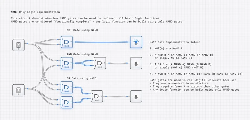
The NAND gate is functionally complete: AND, OR, NOT, XOR, and memory cells all build from NAND alone. CMOS economics make it the dominant standard cell.

TL;DR: A NAND gate outputs 1 unless all inputs are 1 (). It is functionally complete — every other Boolean function can be implemented with NAND gates alone. In CMOS silicon, NAND uses fewer transistors and switches faster than NOR, which is why it dominates modern standard-cell libraries and why “NAND Flash” carries the name.
A 74HC00 IC from any electronics distributor holds four NAND gates in a 14-pin DIP package and costs a few cents. Yet this unassuming chip — and the billions of NAND gates etched into every modern processor — represents the most manufactured logic structure in the history of engineering.
This post focuses on the NAND gate as a practical, physical component: how it is built in CMOS silicon, which real ICs implement it, what their datasheets tell you, and why semiconductor economics made the NAND gate the dominant building block for commercial digital systems.
The NAND Gate: Quick Review
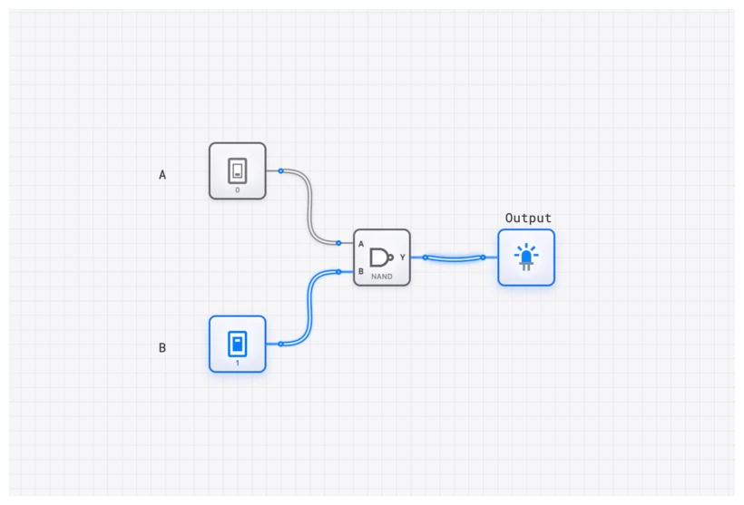
At its core, a NAND gate is an AND gate followed by a NOT gate. It takes two or more inputs and produces a HIGH output (1) unless all inputs are simultaneously HIGH, in which case the output is LOW (0).
Truth Table
| Input A | Input B | Output Y |
|---|---|---|
| 0 | 0 | 1 |
| 0 | 1 | 1 |
| 1 | 0 | 1 |
| 1 | 1 | 0 |
Boolean Expression
By De Morgan’s theorem, this is equivalent to , revealing the NAND gate’s dual nature as an OR gate with inverted inputs.
CMOS Implementation: Why NAND is Silicon’s Natural Gate
To understand why NAND dominates commercial IC design, you need to look at the transistor level. In CMOS technology, every logic gate consists of two complementary networks:
- Pull-Down Network (PDN): NMOS transistors connecting the output to ground ().
- Pull-Up Network (PUN): PMOS transistors connecting the output to the supply voltage ().
For a 2-input NAND gate, the PDN has two NMOS transistors in series, and the PUN has two PMOS transistors in parallel. This arrangement has a critical advantage: NMOS transistors (which use electrons as charge carriers) are inherently faster than PMOS transistors (which use holes). By placing the faster NMOS transistors in series and the slower PMOS transistors in parallel, the NAND gate achieves balanced rise and fall times with minimal transistor sizing.
Compare this to a NOR gate, where the PMOS transistors are in series. Series PMOS transistors add resistance, slowing the pull-up transition and requiring wider (larger) transistors to compensate. This is why, in CMOS, a 2-input NAND gate requires only 4 transistors and occupies less silicon area than an equivalent NOR gate.
An AND gate, by contrast, requires a NAND gate followed by an inverter — 6 transistors total. This 50% transistor overhead is why synthesis tools in the ASIC design flow prefer NAND-based implementations wherever possible.
Real ICs: The 74HC00 and CD4011
The NAND gate has been available as a discrete IC since the earliest days of the TTL (Transistor-Transistor Logic) family. Two of the most widely used NAND gate ICs illustrate different technology generations:
The 74HC00: High-Speed CMOS
The 74HC00 is a quad 2-input NAND gate in a 14-pin DIP (or SOIC) package. It belongs to the 74HC (High-speed CMOS) family and is perhaps the most commonly used logic IC in educational and prototyping contexts.
Key datasheet parameters (typical at = 5V, 25 C):
| Parameter | Symbol | Typical Value |
|---|---|---|
| Supply Voltage | 2V to 6V | |
| Propagation Delay (L-to-H) | 9 ns | |
| Propagation Delay (H-to-L) | 9 ns | |
| Output Current (source) | -4 mA | |
| Output Current (sink) | 4 mA | |
| Quiescent Current | 1 uA | |
| Fan-out (to 74HC inputs) | — | ~10 |
Pin Diagram (14-pin DIP):
- Pins 1, 2 -> Gate 1 inputs; Pin 3 -> Gate 1 output
- Pins 4, 5 -> Gate 2 inputs; Pin 6 -> Gate 2 output
- Pins 9, 10 -> Gate 3 inputs; Pin 8 -> Gate 3 output
- Pins 12, 13 -> Gate 4 inputs; Pin 11 -> Gate 4 output
- Pin 7 -> GND; Pin 14 ->
The CD4011: Classic CMOS
The CD4011 is the CMOS counterpart from the 4000-series family. It has a wider supply voltage range (3V to 18V) but slower propagation delay (typically 50-125 ns at 5V). Its advantage is ultra-low power consumption and tolerance for a wide range of supply voltages, making it popular in battery-powered and industrial applications.
When to use which:
- Use the 74HC00 for breadboard projects and anything synchronized to a clock above 1 MHz.
- Use the CD4011 for low-power, wide-voltage-range applications where speed is not critical.
Timing Specifications: Reading the Datasheet
For any serious design work, the propagation delay numbers from the datasheet are your constraints. Let’s walk through what these numbers mean in practice.
A 74HC00 gate has a typical of 9 ns. If you chain three NAND gates (for example, to build an OR gate using the NAND-only construction), the total delay is approximately ns for the critical path (the signal passes through the input inverter and the final NAND, not all three gates serially for every input).
At 50 MHz (a 20 ns clock period), this leaves only 2 ns of timing margin. At 100 MHz, the delay exceeds the clock period entirely. This is why high-speed designs use dedicated OR cells from standard cell libraries rather than constructing them from discrete NAND gates.
Common Pitfall: Propagation Delay Stacking
When building everything from NAND gates, delays accumulate at each stage. A NAND-based OR gate has a critical path delay of . A NAND-based XOR has a critical path of (three gate levels). In a complex circuit, these stacked delays can limit maximum clock frequency and introduce timing hazards — momentary incorrect outputs called glitches that occur when signals on different paths arrive at different times.
Verification with the OSCILLOSCOPE
To observe propagation delay stacking in digisim.io, build a NAND-based OR gate (three NAND gates) and a native OR gate side by side. Feed the same CLOCK signal to both circuits. Connect three OSCILLOSCOPE channels: one to the CLOCK input, one to the native OR output, and one to the NAND-based OR output.
You will see that both outputs track the clock, but the NAND-based version is shifted further to the right. That additional horizontal offset is the delay tax you pay for using NAND-only construction.
Open NAND Universal Logic Template
Manufacturing Advantages: Why NAND Won the Silicon War
The dominance of the NAND gate in IC manufacturing is not an accident. It stems from three interrelated advantages:
1. Transistor Count
A 2-input NAND gate uses 4 transistors. An AND gate requires 6 (NAND + inverter). An OR gate requires 6 (two inverters + NAND). When you are fitting 10 billion transistors on a die, a 33% reduction in gate-level transistor count translates directly into smaller die area, higher yield, and lower cost per chip.
2. Speed
Because the NMOS pull-down network (the speed-critical path for NAND) has transistors in series with only moderate resistance, and the PMOS pull-up network has transistors in parallel (low resistance), the NAND gate achieves faster switching than the equivalent NOR gate. In advanced process nodes (7 nm, 5 nm, 3 nm), this speed advantage compounds across billions of gates.
3. Standard Cell Libraries
Modern chip design relies on standard cell libraries — pre-characterized gate layouts provided by the foundry. These libraries are heavily NAND-biased. A typical library might offer NAND2, NAND3, NAND4, and even NAND2X2 (double-drive-strength NAND) cells, each optimized for area, speed, and power. The EDA synthesis tool maps your RTL (Register-Transfer Level) design onto these cells, and the optimizer naturally gravitates toward NAND-based implementations because they offer the best area-delay-power product.
Real-World Applications
NAND Flash Memory
The most famous application carries the name itself: NAND Flash. In NAND Flash memory, floating-gate transistors are connected in series — the same topology as the NMOS pull-down network in a NAND gate. This series connection makes NAND Flash denser than NOR Flash (where transistors are in parallel), enabling the massive storage capacities of modern SSDs, USB drives, and smartphones.
ASIC Address Decoders
Inside a processor, address decoders determine which memory location or peripheral is being accessed. A multi-input NAND gate naturally implements the “match this exact bit pattern” function. For a 4-bit address 1101, the decoder inverts the third bit (the 0) and feeds all four lines into a 4-input NAND. The output goes LOW only when the address matches exactly — a compact, fast implementation that scales well in CMOS.
Hands-On: Building a HALF_ADDER from NAND Gates
The 5-NAND-gate HALF_ADDER is a classic design exercise that ties together universality and practical gate economy.
A HALF_ADDER needs two outputs: Sum () and Carry (). The XOR function alone takes 4 NAND gates, and the AND function takes 2. Naively, that is 6 gates. But by sharing an intermediate signal, you can do it in 5:
- Gate 1: Inputs A and B. Output is .
- Gate 2: Inputs A and . Output is .
- Gate 3: Inputs B and . Output is .
- Gate 4: Inputs and . Output is the Sum ().
- Gate 5: Inputs and (tied together). Output is the Carry ().
Gate 5 is simply an inverter applied to , which is . Inverting it yields — the carry. Gate 1’s output () is shared between the XOR construction and the carry path, saving one gate.
Build this on digisim.io and verify both outputs against the half-adder truth table. Use the OSCILLOSCOPE to confirm that the Sum output has a slightly longer delay than the Carry output (three gate levels vs. two).
Curriculum Connection
This post connects to:
- The Unsung Hero: How the NOR Gate Built Apollo — the alternative universal gate.
- Propagation Delay — how delay stacking affects real designs.
- The SR Latch — NAND-based memory cells and the foundation of flip-flops.
Your Challenge
Build a 2-to-1 MULTIPLEXER using only NAND gates. The Boolean expression is . With De Morgan’s transformations, you can implement this entirely in NAND. Count your gates and measure the critical path delay with the OSCILLOSCOPE.