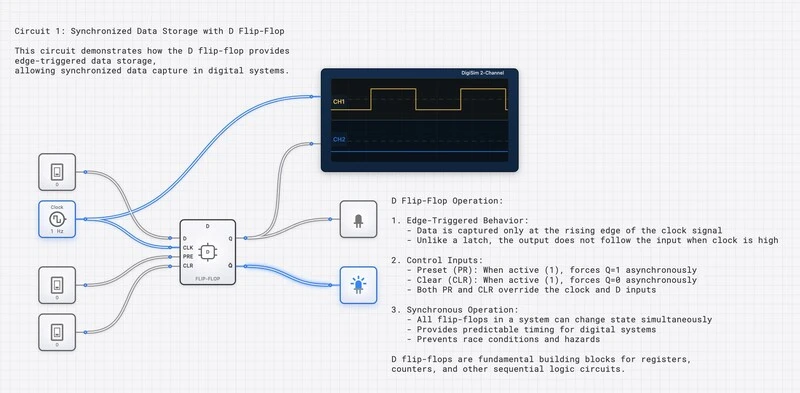
The D Flip-Flop: Edge-Triggered Memory in Digital Design
The D flip-flop captures its D input on a single clock edge — the snapshot behavior every synchronous register needs. Covers timing and metastability.

TL;DR: A D flip-flop captures whatever is on its data (D) input at the moment of an active clock edge and holds that value until the next active edge. Its characteristic equation is . Unlike a D latch, which is transparent while enable is high, the D flip-flop’s capture window is effectively zero — making it the bedrock of synchronous digital design.
Combinational gates — AND, OR, NOT — compute, but they do not remember. To hold a state, you need a memory element. The simple D latch provides storage but with a critical flaw: transparency. A D latch with its Enable held high acts like an open window — any glitch on the input races directly to the output.
For robust, predictable systems we need a component that behaves less like a window and more like a camera, capturing a perfect snapshot of data at one precise instant. That component is the D_FLIP_FLOP, the bedrock of modern synchronous design.
The D_FLIP_FLOP: A Definition
A D_FLIP_FLOP is a synchronous, 1-bit memory element. The “D” stands for “Data,” as its primary purpose is to capture the value present on its data line. Unlike its cousin, the D_LATCH, which is level-sensitive, the D_FLIP_FLOP operates under the strict command of a clock signal’s transition.
In the digisim.io environment, you will find the D_FLIP_FLOP under the Sequential Logic category. It features four essential terminals that you must master:
- D (Data): The input that holds the bit value (0 or 1) you want to store.
- CLK (Clock): The control signal. The flip-flop only acts when it sees a specific transition—an edge—on this input.
- Q: The primary output, reflecting the currently stored bit.
- (Q-bar): The inverted output, which is always the logical opposite of Q.
The magic of the D_FLIP_FLOP lies in its edge-triggered behavior, and understanding this distinction from level-sensitive devices like the D_LATCH is critical:
- Level-sensitive (D Latch): The output follows the input for the entire duration that Enable is high. The “capture window” is as wide as the Enable pulse. Any glitch during that window passes through.
- Edge-triggered (D Flip-Flop): The output captures the input only at the instantaneous transition of the clock—a rising edge (low-to-high) or falling edge (high-to-low). The capture window is effectively zero width. Between edges, the input is completely ignored.
This distinction is the fundamental shift from basic sequential logic to robust synchronous design. A D Latch is transparent; a D Flip-Flop is opaque except for a single, precisely defined instant.
Truth Table: Capturing the Instant
The behavior of a positive-edge-triggered D_FLIP_FLOP can be summarized with a simple but powerful truth table. The arrow () signifies the rising clock edge—the only moment that truly matters in a synchronous system.
| CLK | D | Action | |
|---|---|---|---|
| 0 | 0 | Capture the ‘0’ | |
| 1 | 1 | Capture the ‘1’ | |
| 0 | X | Q | Hold state (Static) |
| 1 | X | Q | Hold state (Static) |
| X | Q | Hold state (Falling edge ignored) |
The ‘X’ in the D column is a “don’t care” symbol. It signifies that as long as the CLOCK is not transitioning, the D input has no effect on the output Q. The output simply maintains its last captured value. This is why we call it “edge-triggered.” If you are debugging a circuit and the output isn’t changing when you flip a switch, check your CLOCK. Is it pulsing? If not, the D_FLIP_FLOP is doing exactly what it was designed to do: nothing.
The Underlying Logic: The Characteristic Equation
While we can build a D_FLIP_FLOP from gates—typically using a master-slave configuration of two D_LATCH components—its behavior is most elegantly described by its characteristic equation. This equation defines the next state of the output, denoted as , based on the current input, D.
For a D_FLIP_FLOP, the equation is beautifully simple:
This equation reads: “The value of Q after the next clock edge will be whatever the value of D is at that clock edge.”
The D_FLIP_FLOP is the “copycat” of the digital world. It doesn’t perform logic; it just remembers. But by chaining these copycats together, we create the 4-bit register, the shift register, and eventually the entire memory hierarchy of a CPU.
Common Pitfall: The Metastability Minefield
A flip-flop seems like a perfect digital device, but it lives in an analog world. Its promise of capturing data at a precise instant comes with a strict contract, defined by two timing parameters: Setup Time and Hold Time.
- Setup Time (): This is the minimum time the D input must be stable before the active clock edge arrives. The flip-flop needs this time to “see” the data and prepare the internal gates for capture.
- Hold Time (): This is the minimum time the D input must remain stable after the active clock edge has passed. The internal circuitry needs this time to reliably lock the value.
What happens if you violate this contract? You enter the realm of metastability.
Imagine a ball balanced perfectly on the peak of a steep roof. It wants to fall to the left (0) or the right (1), but for a brief, unpredictable moment, it teeters in the middle. In a digital circuit, if the D input changes within the critical setup-and-hold window, the output Q can exhibit one of several failure modes:
- Intermediate voltage: Q settles at a voltage between valid HIGH and LOW thresholds. Downstream gates may interpret this differently, with some reading ‘0’ and others reading ‘1’ from the same signal.
- Prolonged oscillation: The internal feedback loop oscillates between states before eventually resolving—but the resolution time is probabilistic, not deterministic.
- Delayed resolution: Q eventually settles to a valid state, but the delay exceeds the clock period, causing the next stage to sample stale or invalid data.
The standard engineering countermeasure for asynchronous inputs (signals that have no timing relationship to the system clock) is the two-stage synchronizer: two D_FLIP_FLOPs in series, both clocked by the system clock. The first flip-flop may go metastable, but it has a full clock period to resolve before the second flip-flop samples its output. This reduces the probability of metastability propagating to astronomically low levels.
In a complex system like a modern CPU, a single unresolved metastable event can cause catastrophic failure. This is why we use the OSCILLOSCOPE_8CH in digisim.io to verify timing relationships—ensuring data is stable well before the clock edge arrives.
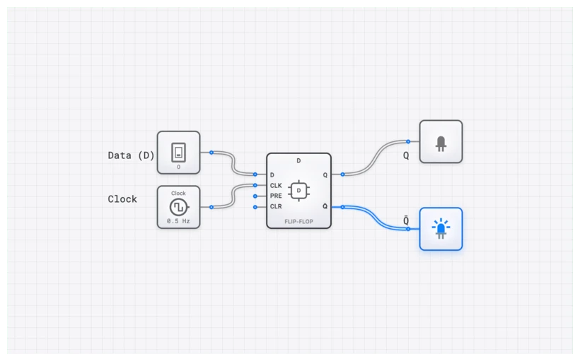
Interactive Simulation: Building the Edge-Triggered D_FLIP_FLOP
Let’s move from theory to the canvas. To truly understand the difference between a level-sensitive latch and an edge-triggered flip-flop, you need to see them side-by-side.
Step-by-Step Simulation Guide
- Open the Workspace: Navigate to the digisim.io editor.
- Place the Components:
- Drag a D_FLIP_FLOP onto the canvas.
- Add an INPUT_SWITCH for the D input.
- Add a CLOCK component for the CLK input.
- Add an OUTPUT_LIGHT to the Q output.
- The Test:
- Turn the INPUT_SWITCH to ‘1’. Notice the OUTPUT_LIGHT stays off.
- Toggle the CLOCK. The moment the clock goes from 0 to 1, the light turns on.
- Now, turn the INPUT_SWITCH to ‘0’ while the clock is still high (1). Notice the light stays on! This is the key difference from a D_LATCH. The flip-flop is no longer “transparent.” It captured the ‘1’ at the rising edge and is now ignoring the fact that the input has changed.
- Verification with OSCILLOSCOPE:
- Connect Channel 1 of an OSCILLOSCOPE to the CLOCK.
- Connect Channel 2 to the Q output.
- Run the simulation and observe the waveforms. You will see that the Q output only transitions in perfect synchronization with the rising edge of the clock.
Real-World Applications: From Registers to Frequency Dividers
The D_FLIP_FLOP isn’t just an academic exercise; it is the fundamental building block of every digital device you’ve ever used.
1. CPU Registers and the ACCUMULATOR
A 64-bit processor contains numerous registers. A 64-bit register is essentially an array of 64 D_FLIP_FLOP components, all sharing a common CLOCK line. When the CPU executes an instruction to “store” a result, it places the data on the DATA_BUS_8BIT (or 64-bit equivalent) and pulses the clock. In that single, synchronous instant, the entire value is captured. This is exactly how the ACCUMULATOR and INSTRUCTION_REGISTER function in our CPU architecture lessons (Lessons 63-70).
2. Frequency Dividers
If you take a D_FLIP_FLOP and connect its inverted output () back to its own D input, you create a toggle circuit.
On every rising clock edge, the flip-flop captures the opposite of its current state. If Q was 0, it becomes 1. If it was 1, it becomes 0. Because it takes two clock pulses to complete a full cycle (0 1 0) on the Q output, the output frequency is exactly half of the input clock frequency. This is the basis for digital watches and baud rate generators in serial communication.
Why Synchronous Design Wins
Before the D_FLIP_FLOP became standard, engineers struggled with “asynchronous” designs where signals wandered through gates at different speeds, causing “glitches” or “races.”
By using the D_FLIP_FLOP, we enforce a global heartbeat—the CLOCK. We allow the combinational logic (the AND and OR gates) to be messy and have propagation delays (), as long as they settle down before the next clock edge arrives. The D_FLIP_FLOP acts as a barrier, preventing that messiness from propagating through the system. It creates a “safe harbor” for data.
This is why we spend so much time on Sequential Logic in our curriculum (Lessons 41-62). Once you master the D_FLIP_FLOP, you understand how time itself is managed in a computer.
Summary and Next Steps
We’ve covered a lot of ground. We’ve moved from the “transparent” danger of latches to the “snapshot” precision of the D_FLIP_FLOP. We’ve looked at the characteristic equation , and we’ve faced the reality of metastability and timing constraints.
For the next steps in sequential logic, read The JK Flip-Flop (which adds toggle, set, and reset modes), then SR vs. JK Flip-Flops. For the timing physics behind the contract you just learned, read The Unseen Clock.
Your Challenge: Try to build a 4-bit register. Use four D_FLIP_FLOP components, connect all their CLK pins to a single CLOCK, and store a 4-bit nibble (like 1011) simultaneously. Use SimCast to record the circuit in action — it’s the best way to spot timing issues the naked eye misses.