The Clock Pulse: Why Computers Need a Heartbeat
The clock signal is the periodic square wave that synchronizes every flip-flop in a synchronous system. Covers frequency, duty cycle, skew, and jitter.

TL;DR: A clock signal is a periodic square wave (typically 50% duty cycle) that synchronizes every flip-flop and pipeline stage in a synchronous digital system. Modern CPUs derive multi-GHz clocks from low-frequency crystal oscillators using phase-locked loops, then distribute them through balanced clock trees while managing skew and jitter.
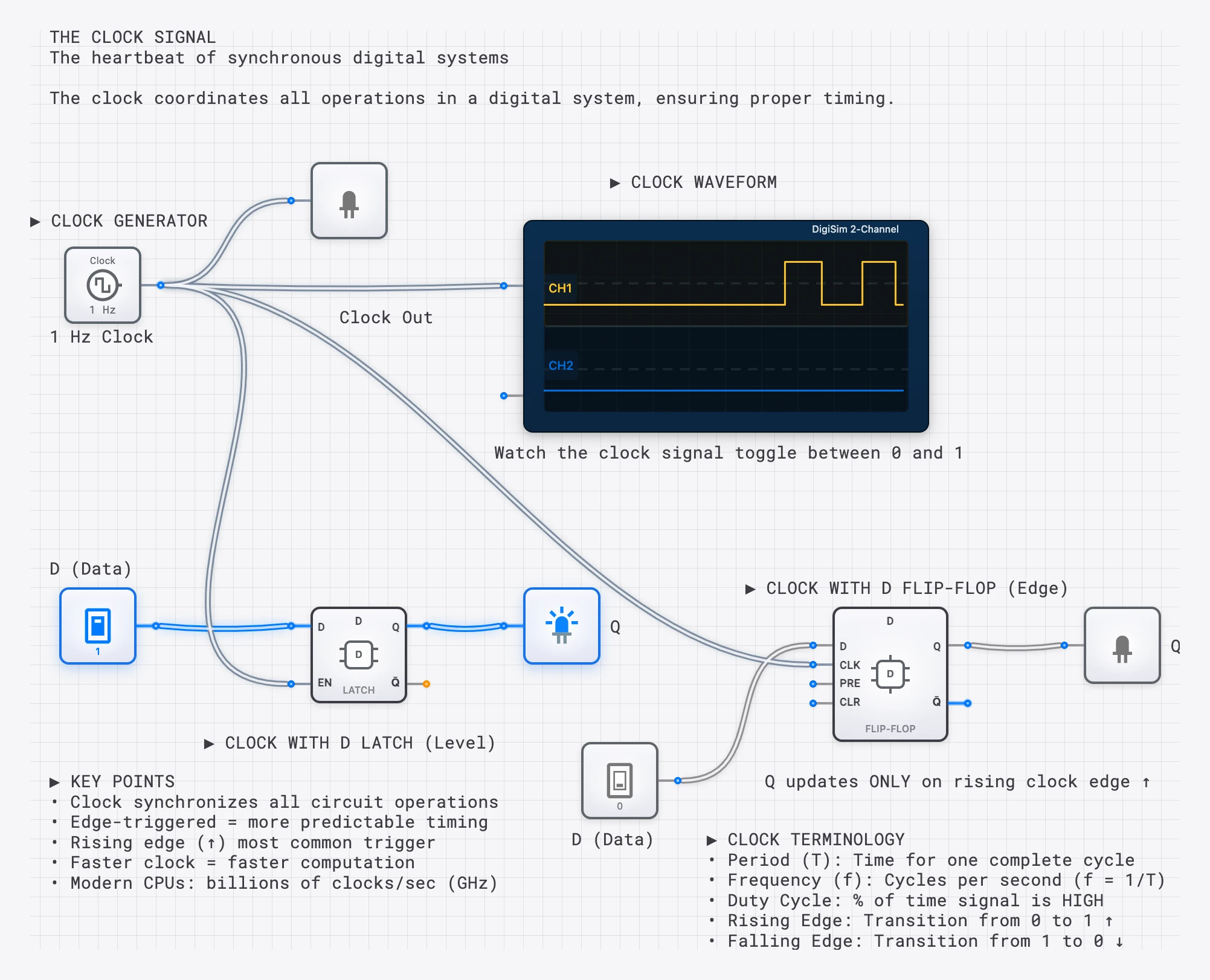
Every digital computer has a pulse — a rhythmic signal that coordinates billions of operations with precise timing. This is the clock signal, and it is what transforms a collection of logic gates into a functioning computer. Without it, signals arriving at different times through different combinational paths would produce garbled results.
What is a Clock Signal?
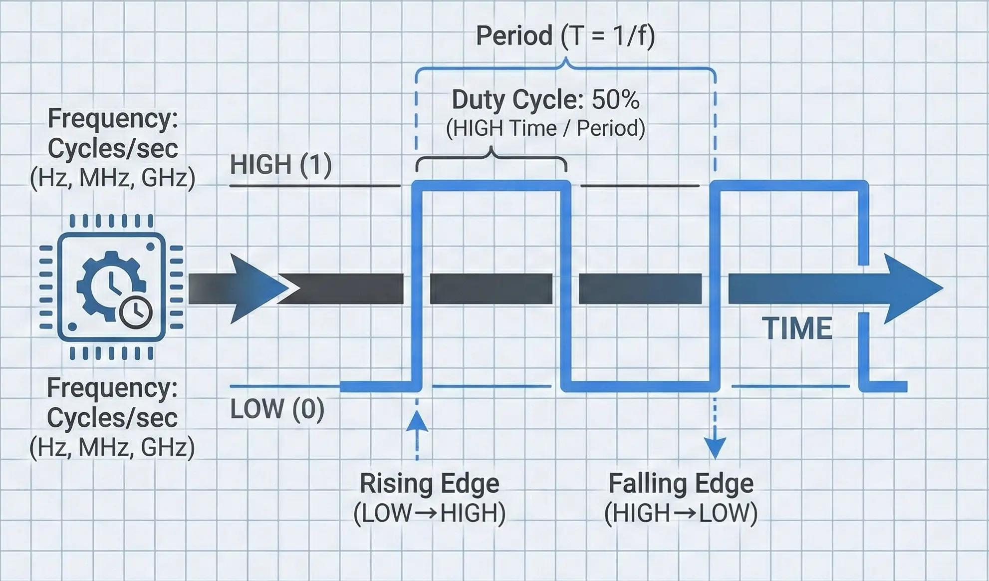
A clock signal is a periodic square wave that oscillates between HIGH (1) and LOW (0) at a fixed frequency. It serves as the master timing reference for all synchronous operations in a digital system. Every flip-flop, every register, every pipeline stage in a processor listens to this signal and acts only when it commands.
Clock Signal Properties
A clock signal is defined by four fundamental properties:
Frequency (): The number of complete cycles per second, measured in Hertz (Hz). A 3.5 GHz processor clock completes 3.5 billion cycles every second.
Period (): The time for one complete cycle. Period and frequency are reciprocals:
At 3.5 GHz, each clock cycle lasts approximately 0.286 nanoseconds—light travels about 8.6 centimeters in that time.
Duty Cycle: The percentage of each period during which the signal is HIGH. A 50% duty cycle means the signal spends equal time HIGH and LOW. While 50% is the ideal and most common, some designs use asymmetric duty cycles for specific timing requirements.
A duty cycle significantly different from 50% can cause problems in designs that use both rising and falling edges (dual-edge clocking), since the HIGH and LOW phases would have unequal durations for setup and computation.
Edges: The transitions between states. The rising edge (LOW to HIGH) and falling edge (HIGH to LOW) are the precise instants at which synchronous circuits act. Most digital systems trigger on the rising edge, though some use the falling edge or both.
Why Do We Need a Clock?
1. Synchronization
Digital circuits are built from physical components with finite propagation delays—signals take time to travel through gates and along wires. An AND gate might settle in 2 nanoseconds while a multi-bit adder might take 15 nanoseconds. Without a clock, different signals would arrive at their destinations at different times, causing circuits to compute with partially-updated data.
The clock solves this by enforcing a simple rule: no circuit is allowed to use a result until the next clock edge. As long as all signals settle before that edge arrives, the system produces correct results. It does not matter that different paths have different delays, as long as the slowest path finishes within one clock period.
Think of the clock as an orchestra conductor. Each musician (gate) may play at a different tempo, but the conductor’s baton ensures everyone starts each measure together. Without the conductor, you get cacophony instead of symphony.
2. Sequential Logic
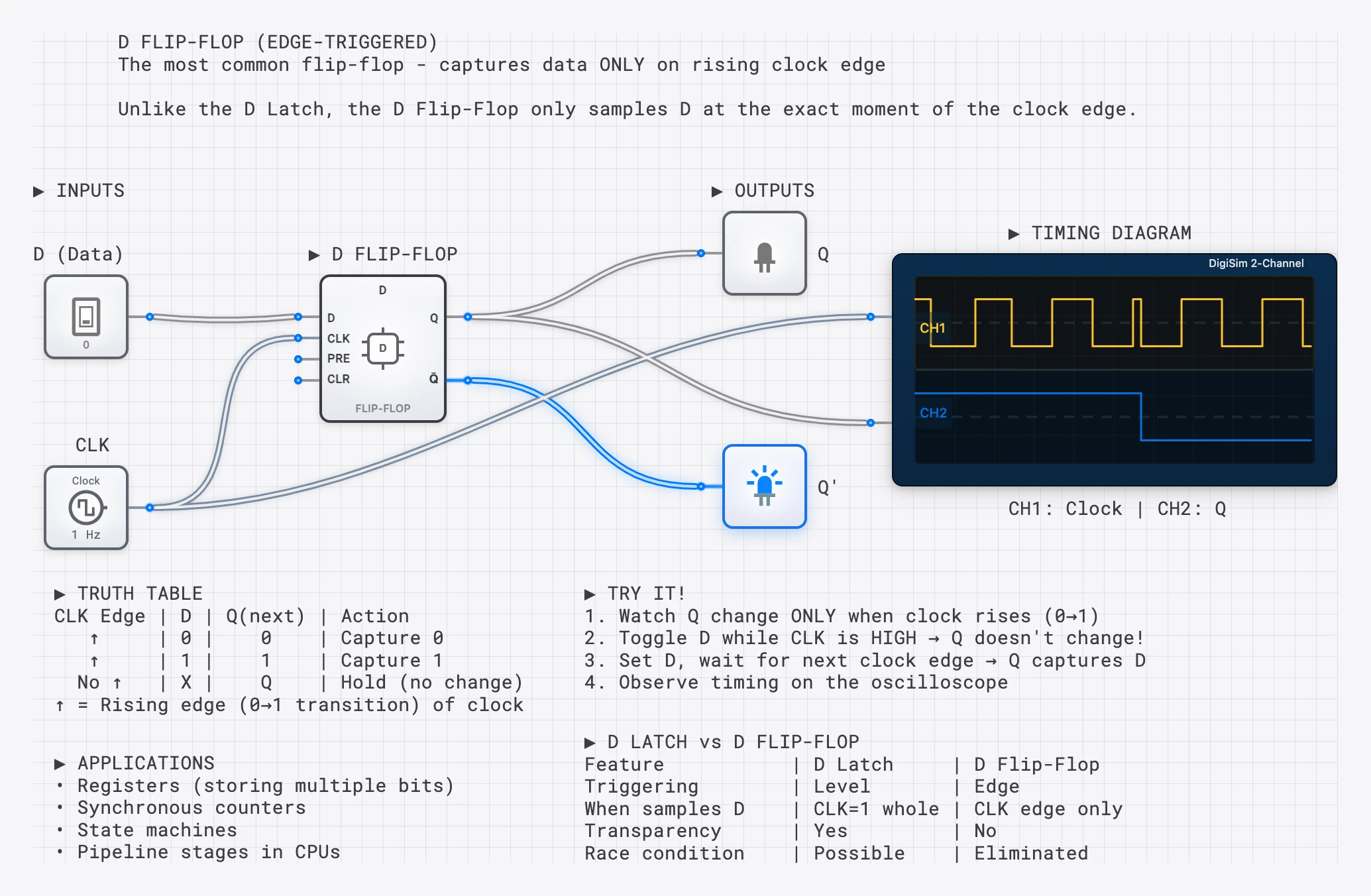
Flip-flops and registers need to know when to capture new data. The clock’s edge provides that precise command: “Now. Capture whatever value is on the input.” This is what makes memory, state machines, and computation possible. See The D Flip-Flop for a deep dive on edge-triggered capture, or The T Flip-Flop for clock-driven counting.
3. Pipeline Coordination
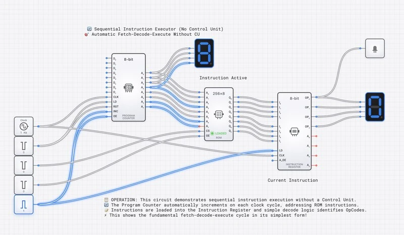
Modern CPUs use pipelining—breaking instructions into stages (Fetch, Decode, Execute, Write-back) that execute in parallel, like an assembly line. The clock advances data through each pipeline stage simultaneously. On each tick, every stage passes its result forward and receives new work from the stage behind it. Without the clock’s coordination, pipeline stages would overwrite each other’s data.
Clock Speed and Performance
A CPU’s clock speed (e.g., 3.5 GHz) tells you how many cycles occur per second. Faster clocks generally mean faster processing—but with important physical limits.
| Era | Example CPU | Clock Speed | Context |
|---|---|---|---|
| 1971 | Intel 4004 | 740 kHz | First microprocessor |
| 1982 | Intel 80286 | 6-12 MHz | IBM PC AT era |
| 1993 | Intel Pentium | 60-66 MHz | Superscalar design |
| 2000 | AMD Athlon | 1 GHz | First 1 GHz consumer CPU |
| 2024 | Modern Desktop | 4-5+ GHz | Multi-core, turbo boost |
The Power Wall
Clock speed hit a practical ceiling around 2004-2006 at roughly 3-4 GHz. The reason is thermodynamic: power consumption scales with frequency, and at high frequencies, the heat generated exceeds what can be reasonably dissipated. The relationship is approximately:
where is capacitance, is voltage, and is frequency. Doubling the frequency roughly doubles the power consumption (and heat output). This is why the industry shifted from “faster clocks” to “more cores”—it is more efficient to run four cores at 3 GHz than one core at 12 GHz.
Overclocking: Pushing the Limits
Overclocking is the practice of running a processor’s clock faster than its rated speed. When it works, you get faster computation. When it fails, the clock period becomes shorter than the critical path delay through the logic, meaning signals have not settled when the next clock edge arrives. The flip-flops capture invalid data, and the system crashes—the infamous “Blue Screen of Death” in overclocked PCs. Overclocking is a direct, practical demonstration of the timing constraints we discuss in setup and hold time analysis.
How Clock Signals Are Generated
Clock signals do not appear from nowhere. They are generated by specialized circuits, each with different tradeoffs in precision, cost, and flexibility.
Crystal Oscillators
The most common clock source in digital systems is the crystal oscillator. A thin slice of quartz crystal vibrates at a precise mechanical frequency when an electric field is applied (the piezoelectric effect). This vibration generates an extremely stable electrical signal.
Crystal oscillators are valued for their accuracy—typically within 20-50 parts per million (ppm), meaning a 10 MHz crystal drifts by at most 500 Hz. This is why they are used as the master timing reference in everything from microcontrollers to digital watches. The famous 32.768 kHz “watch crystal” vibrates at exactly Hz, making it trivial to divide down to 1 Hz using a chain of T flip-flops.
Phase-Locked Loops (PLLs)
Most processors do not run at the crystal’s native frequency. Instead, they use a Phase-Locked Loop (PLL) to multiply the crystal frequency up to the desired clock speed. A PLL is a feedback control system that:
- Takes a low-frequency reference signal (from the crystal).
- Generates a high-frequency output signal.
- Continuously adjusts the output to maintain a fixed phase relationship with the reference.
For example, a motherboard might use a 100 MHz crystal reference and a PLL with a multiplication factor of 35 to produce a 3.5 GHz CPU clock. PLLs can also generate multiple derived clocks at different frequencies for different subsystems (memory, I/O bus, etc.).
Ring Oscillators
A ring oscillator is the simplest clock generator: an odd number of inverters connected in a loop. The signal propagates around the ring, inverting at each stage, creating a self-sustaining oscillation. The frequency depends on the number of stages and the propagation delay of each inverter:
where is the number of inverters and is the propagation delay of each. Ring oscillators are not precise enough for system clocks, but they are useful for on-chip delay measurement and testing. In digisim.io, you can build one by connecting an odd number of NOT gates in a loop.
Clock Distribution: Getting the Signal Everywhere
Generating a clean clock signal is only half the challenge. The other half is distributing it to every flip-flop in the system with minimal timing variation. In a modern processor with billions of transistors spread across a chip, this is a serious engineering problem.
The Clock Tree
A clock tree is a hierarchical network of buffers (amplifiers) arranged to deliver the clock signal from a single source to every flip-flop with equal delay. The tree structure ensures that:
- Each branch point splits the signal into two or more paths.
- Buffers at each level restore signal strength.
- Wire lengths are carefully balanced so the clock arrives at all destinations simultaneously.
Designing the clock tree is one of the most critical tasks in chip design. A modern CPU’s clock tree can consume 30-40% of the chip’s total power budget just to distribute the timing signal.
Clock Skew
Clock skew is the difference in arrival time of the clock signal at two different flip-flops in the same system. If flip-flop A receives the clock 0.5 ns before flip-flop B, the skew between them is 0.5 ns. Skew is caused by:
- Unequal wire lengths in the distribution network.
- Variations in buffer delay due to manufacturing tolerances.
- Temperature gradients across the chip (hotter regions have slower gates).
Excessive skew is dangerous because it can cause one flip-flop to capture data from the “wrong” clock cycle. If the skew exceeds the hold time margin, a register might see data that has already been updated by the source register—a hold time violation.
Clock Jitter
Clock jitter is the random, cycle-to-cycle variation in the clock period. While skew is a spatial problem (different locations receive the clock at different times), jitter is a temporal problem (the same location receives clock edges with slightly varying intervals).
Jitter comes from noise in the oscillator circuitry, power supply fluctuations, and electromagnetic interference. It directly reduces the timing margin available for computation, since the “worst-case” clock period is shorter than the nominal period by the amount of the jitter.
In high-speed designs, managing jitter down to picosecond levels is critical.
Edge-Triggered Operations
Most synchronous operations occur on a specific clock edge—the instant of transition. This is far more precise than reacting to the signal level.
Rising Edge (positive edge): The moment the clock goes from 0 to 1. This is the most common trigger in digital design.
Falling Edge (negative edge): The moment the clock goes from 1 to 0. Used in some designs and in master-slave flip-flop architectures.
Dual-Edge: Some high-performance designs (like DDR memory) trigger on both edges, effectively doubling the data rate without increasing the clock frequency. DDR stands for “Double Data Rate” precisely because it transfers data on both the rising and falling edges.
Clock in CPU Operations
Every CPU instruction takes a specific number of clock cycles to complete. This is the instruction’s latency, measured in Cycles Per Instruction (CPI). A simple register-to-register ADD might complete in 1 cycle, while a cache miss that requires fetching data from main memory might stall the pipeline for 100+ cycles.
The overall performance of a processor is determined by three factors:
This equation reveals why clock speed alone does not determine performance. A processor with a slower clock but lower CPI (more work per cycle) can outperform a faster-clocked processor with higher CPI. This is the fundamental tradeoff between clock frequency and architectural efficiency that defines modern processor design.
The Relationship Between Clock and Timing Constraints
The clock period sets a hard budget for how much computation can happen between clock edges. For a signal traveling from flip-flop A through combinational logic to flip-flop B:
where:
- is the clock-to-Q delay of the source flip-flop.
- is the worst-case delay through the combinational logic (the critical path).
- is the setup time of the destination flip-flop.
If the clock period is shorter than this sum, the destination flip-flop will sample data before it has settled—a setup time violation that produces incorrect results. The longest such path in the entire design is the critical path, and it determines the maximum achievable clock frequency:
When accounting for real-world imperfections, the timing budget must also include clock skew and jitter:
Every nanosecond consumed by skew and jitter is a nanosecond stolen from the time available for actual computation. This is why clock distribution engineering has such an outsized impact on system performance.
Clock Gating: Saving Power
In a modern processor, the clock tree is the single largest consumer of dynamic power. Every buffer in the tree switches twice per cycle, and there are millions of them. Clock gating is the primary technique for reducing this power consumption.
The idea is simple: if a block of logic is not performing useful work in a given cycle, stop delivering the clock to it. No clock transitions means no switching, which means no dynamic power consumption.
A clock gate is typically implemented as an AND gate (or a specialized latch-based gate to prevent glitches) that combines the system clock with an enable signal:
When Enable is LOW, the gated clock stays LOW, and all flip-flops in the downstream block hold their current values. Modern processors aggressively clock-gate unused functional units, idle cores, and inactive peripherals. A laptop processor might gate over 90% of its clock tree during light workloads, which is a major reason modern chips can achieve reasonable battery life despite containing billions of transistors.
Multiple Clock Domains
Real digital systems rarely operate on a single clock. A modern SoC (System on Chip) might have:
- A CPU core running at 3 GHz
- A GPU at 1.5 GHz
- A memory controller at 800 MHz
- USB interfaces at 480 MHz
- A real-time clock at 32.768 kHz
Each of these is a separate clock domain. Signals crossing between domains have no timing relationship to each other, making them effectively asynchronous. Every such crossing requires a synchronizer (typically two flip-flops in series) to prevent metastability, as discussed in The Unseen Clock: setup, hold, and metastability.
Managing clock domain crossings is one of the most error-prone aspects of modern chip design. It is estimated that clock domain crossing bugs account for a significant fraction of silicon respins (costly chip redesigns) in the industry.
Try It Yourself
Build and explore clock-driven circuits on digisim.io:
- Build a ring oscillator: Connect an odd number of NOT gates in a loop and observe the self-sustaining oscillation on the oscilloscope.
- Clock a flip-flop: Wire a D flip-flop with a clock and verify that the output only changes on the rising edge.
- Frequency divider: Connect a T flip-flop with T=1 to a clock. Use the oscilloscope to confirm the output frequency is exactly half the input.
- 4-bit counter: Chain four T flip-flops to count clock pulses. Observe the binary counting pattern on the oscilloscope.
- Duty cycle experiment: Try generating clocks with different duty cycles and observe how they affect the behavior of edge-triggered vs. level-sensitive circuits.
Once the clock itself is comfortable, the natural next step is timing: read The Unseen Clock for setup/hold/metastability, then Mastering Frequency Division to use the clock to drive counters and timers.