SR vs. JK Flip-Flops: The Basics of Sequential Logic
The JK flip-flop solves the SR latch's forbidden state by redefining J=K=1 as toggle. Compare both, derive excitation tables, and build counters from each.

TL;DR: The SR latch is the simplest memory element but has a forbidden state when both inputs are 1. The JK flip-flop fixes this by redefining J=K=1 as a toggle, using internal feedback (, ) and a master-slave clock to prevent race-around oscillation.
Combinational circuits — adders, multiplexers — produce outputs from current inputs alone. Sequential logic adds memory: a flip-flop holds state across clock cycles. This guide compares the two foundational sequential components — the SR latch and the JK flip-flop — and shows how the JK design eliminates the SR’s critical flaw.
Combinational vs. Sequential Logic
Combinational circuits (like adders and multiplexers) produce outputs based solely on their current inputs. Change the inputs, and the outputs change immediately. Remove the inputs, and the outputs are undefined.
Sequential circuits add a critical property: state. Their outputs depend not only on current inputs but also on the history of inputs—they have memory. A flip-flop can be in state Q=0 or Q=1 and will maintain that state until explicitly told to change. This is what makes computation possible: without state, there are no registers, no counters, no program counters, and no CPUs.
The SR Latch: Where Memory Begins
The SR Latch (Set-Reset Latch) is the simplest memory element, built from two cross-coupled NOR (or NAND) gates. It has two inputs—S (Set) and R (Reset)—and two complementary outputs: Q and .
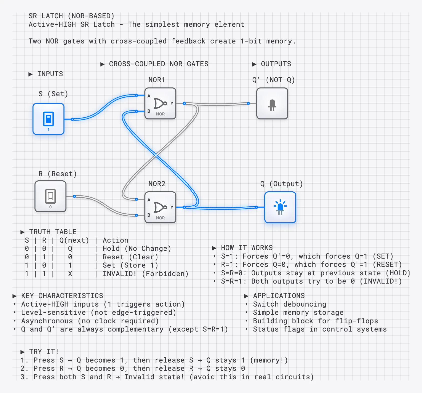
SR Latch Truth Table
| S | R | Q (next) | Action |
|---|---|---|---|
| 0 | 0 | Q (unchanged) | Hold (Memory) |
| 0 | 1 | 0 | Reset (Clear) |
| 1 | 0 | 1 | Set (Store 1) |
| 1 | 1 | ? | INVALID (Forbidden) |
SR Latch Characteristic Equation
The behavior is formally described by:
The constraint is the SR Latch’s fundamental weakness: the equation is only valid when S and R are not both ‘1’. Violating this constraint produces the forbidden state—both outputs go to ‘0’, and the final state upon release is a nondeterministic race condition.
Why the Forbidden State is Dangerous
When S=R=1, both NOR gates are forced to output ‘0’, so Q = = 0—a logical contradiction. When both inputs return to ‘0’ simultaneously, both gates race to output ‘1’. The winner depends on nanosecond-scale differences in propagation delay, temperature, and manufacturing tolerances. The result is unpredictable, and in the worst case, the output can enter a metastable state—an intermediate voltage that is neither a valid ‘0’ nor a valid ‘1’.
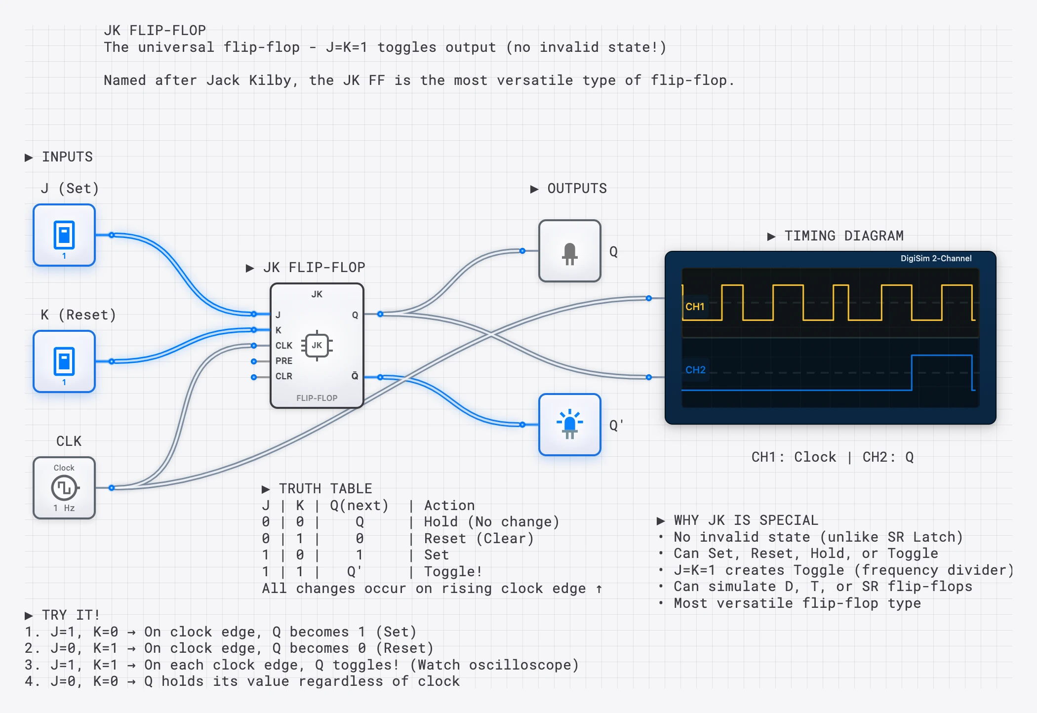
The JK Flip-Flop: The Complete Solution
The JK Flip-Flop confronts the SR Latch’s forbidden state head-on. Rather than leaving the condition undefined, the JK design redefines it as a toggle: the output inverts on each clock edge. This single innovation transforms a flawed memory element into the most versatile flip-flop in digital design.
JK Flip-Flop Truth Table
| J | K | Q (next) | Action |
|---|---|---|---|
| 0 | 0 | Q (unchanged) | Hold |
| 0 | 1 | 0 | Reset |
| 1 | 0 | 1 | Set |
| 1 | 1 | (inverted) | Toggle |
JK Flip-Flop Characteristic Equation
The key difference from the SR equation is the feedback: feeds back into the J term, and Q feeds back into the K term. This internal feedback prevents the race condition—the flip-flop’s current state gates its own inputs, ensuring that only one transition occurs per clock edge.
The Master-Slave Architecture
Early JK designs were level-triggered, which introduced the race-around condition: if the clock pulse was high long enough, the toggled output could feed back and cause another toggle within the same pulse, leading to uncontrolled oscillation.
The solution is the master-slave architecture, which uses two SR latches in series:
- Master latch: Captures input while the clock is HIGH. Its output is isolated from the slave.
- Slave latch: Captures the master’s output when the clock transitions to LOW. This is when the external Q output actually changes.
Because the master and slave are never transparent simultaneously, the output can only change once per clock cycle. Modern implementations use edge-triggering to achieve the same effect more efficiently, but understanding the master-slave concept explains why the JK Flip-Flop needs a clock and why it is immune to the race-around problem.
The Race-Around Condition: A Deeper Look
The race-around condition deserves close attention because it illustrates why clocking strategy matters so much.
In a simple level-triggered JK latch with J=K=1 (toggle mode), the sequence is:
- Clock goes HIGH. The output toggles from 0 to 1.
- The new output (Q=1) feeds back to the input gates.
- The clock is still HIGH. The gate logic sees the new state and toggles again: Q goes from 1 to 0.
- This cycle repeats for as long as the clock remains HIGH.
The output oscillates at the propagation delay frequency of the gates—essentially becoming a ring oscillator. The final state when the clock falls depends on the exact pulse width relative to the gate delay, making the behavior nondeterministic.
Edge-triggered JK Flip-Flops (as used in digisim.io) eliminate this entirely. The flip-flop samples J and K only at the clock transition instant. By the time the output changes and feeds back, the sampling window has already closed.
Excitation Tables: Designing with Flip-Flops
When designing sequential circuits (like counters or state machines), you work backwards from the desired state transitions to determine the required inputs. This is where excitation tables become essential.
SR Latch Excitation Table
| (current) | (desired) | S | R |
|---|---|---|---|
| 0 | 0 | 0 | X |
| 0 | 1 | 1 | 0 |
| 1 | 0 | 0 | 1 |
| 1 | 1 | X | 0 |
(X = don’t care)
JK Flip-Flop Excitation Table
| (current) | (desired) | J | K |
|---|---|---|---|
| 0 | 0 | 0 | X |
| 0 | 1 | 1 | X |
| 1 | 0 | X | 1 |
| 1 | 1 | X | 0 |
Notice the abundance of don’t-care conditions in the JK excitation table. Each transition has one don’t-care, compared to the SR table where don’t-cares are fewer and the constraint must still be enforced. These additional don’t-cares allow for significantly greater Boolean simplification when designing the combinational logic that drives the flip-flops—a tangible advantage when minimizing gate count in real designs.
Comprehensive Comparison
| Feature | SR Latch | JK Flip-Flop |
|---|---|---|
| Inputs | S (Set), R (Reset) | J, K, Clock |
| S=R=1 / J=K=1 | Invalid (race condition) | Toggle (well-defined) |
| Triggering | Level-sensitive (asynchronous) | Edge-triggered (synchronous) |
| Clock required? | No (basic SR latch) | Yes |
| Characteristic equation | ||
| Forbidden state | Exists (S=R=1) | Eliminated |
| Don’t-cares in excitation table | Fewer | More (better optimization) |
| Race-around risk | N/A (no clock) | Eliminated by edge-triggering |
| Gate count | 2 (NOR or NAND) | ~12 (master-slave implementation) |
| Primary use cases | Switch debouncing, SRAM cells | Counters, FSMs, registers |
| Can build other flip-flop types? | Limited | Yes (universal) |
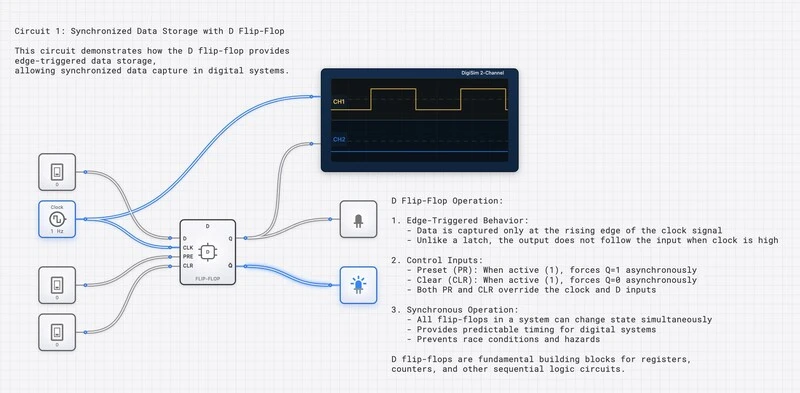
Edge Triggering: The Clock’s Role
Modern flip-flops are edge-triggered—they only change state at the precise moment of a clock transition. This is fundamentally different from the level-sensitive SR Latch, which responds to inputs at any time.
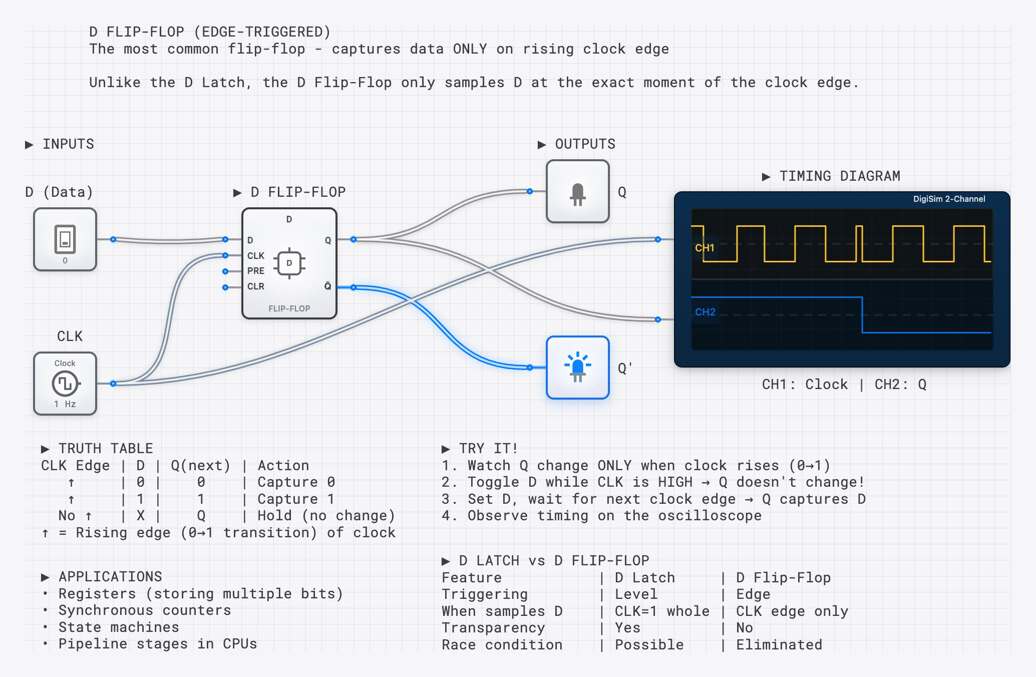
Edge triggering provides three critical guarantees:
- Determinism: The output changes exactly once per clock cycle, at a predictable moment.
- Noise immunity: Input glitches between clock edges are ignored.
- Composability: Multiple flip-flops sharing the same clock update simultaneously, enabling coordinated multi-bit operations.
Converting Between SR and JK
Because the JK Flip-Flop is considered “universal,” it can emulate other flip-flop types. Understanding these conversions deepens your grasp of both components.
SR to JK conversion: Add AND gates that feed back Q and :
The feedback ensures that when J=K=1, only one of S or R is active (depending on the current state), producing the toggle behavior while structurally preventing the forbidden SR state.
JK to D conversion: Connect D to J and to K.
JK to T conversion: Tie J and K together as a single T input.
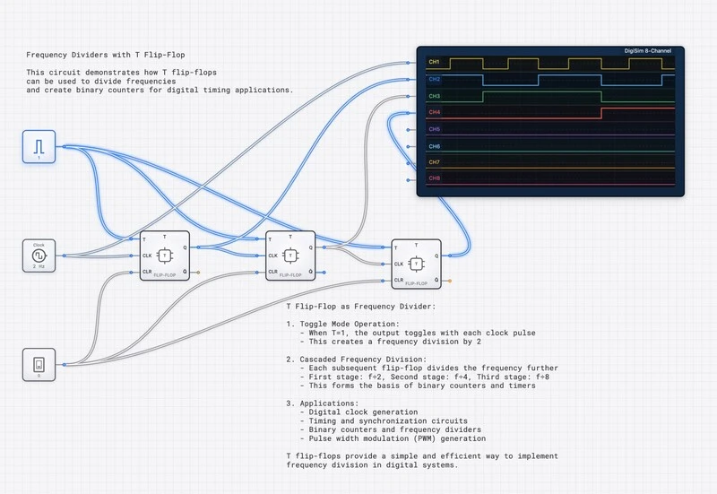
Building Counters: The JK Flip-Flop’s Signature Application
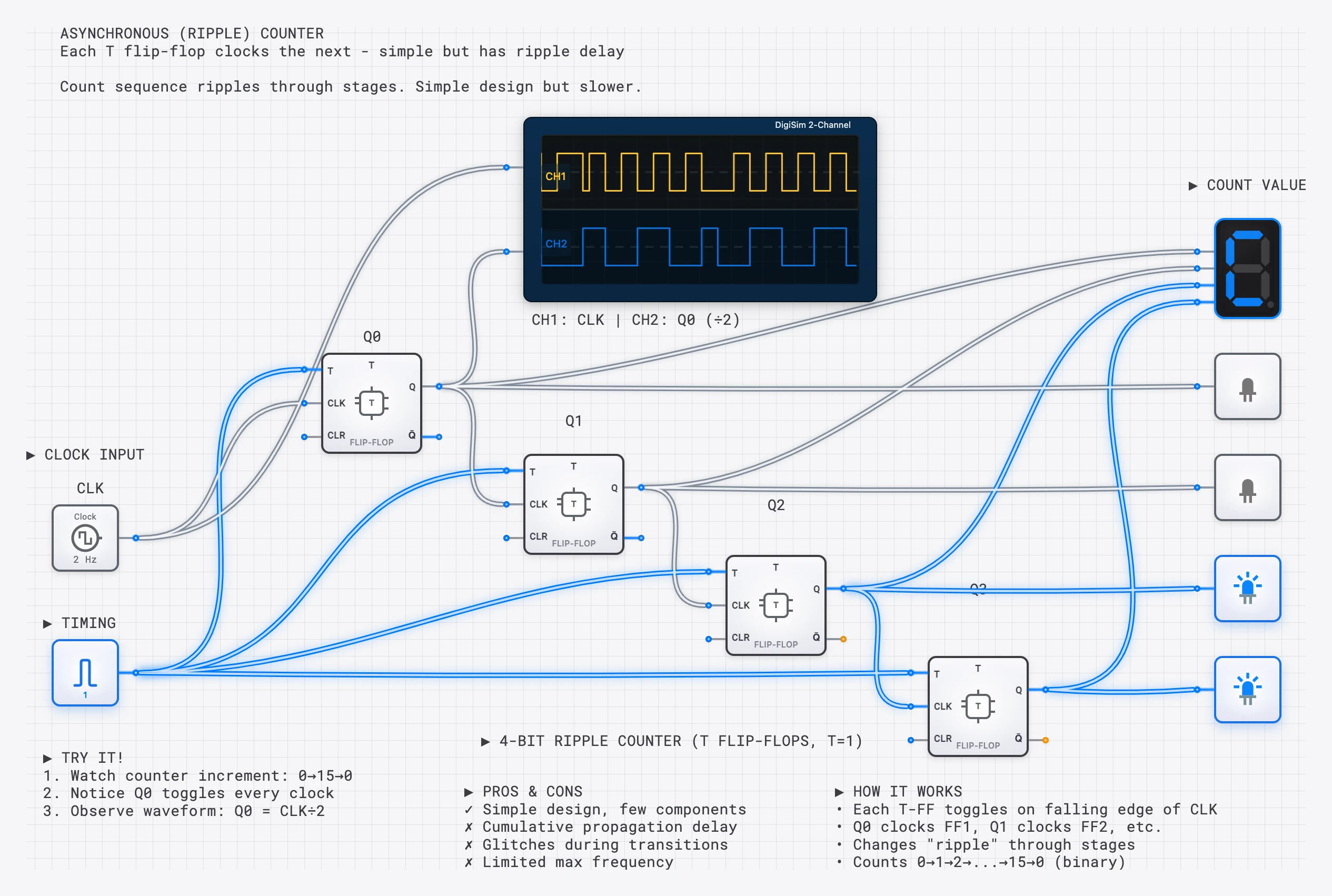
When J=K=1, the JK Flip-Flop toggles on every clock edge—making it the natural building block for binary counters. Chain four JK Flip-Flops with their Q outputs driving the next stage’s clock, and you have a 4-bit ripple counter that sequences through 0000 to 1111.
Ripple Counter (Asynchronous)
In a ripple counter, each flip-flop’s Q output drives the clock input of the next flip-flop. The count “ripples” through the chain as each stage triggers the next:
- FF0 toggles on every system clock edge (frequency = ).
- FF1 toggles on every FF0 transition (frequency = ).
- FF2 toggles on every FF1 transition (frequency = ).
- FF3 toggles on every FF2 transition (frequency = ).
The outputs Q3 Q2 Q1 Q0 represent a 4-bit binary number that increments by 1 on each clock cycle. The tradeoff is that each stage introduces a propagation delay, so the higher-order bits settle later than the lower-order bits. For a brief moment after each clock edge, the counter output may display a transient incorrect value. In high-speed applications, this ripple delay can be problematic, which is why synchronous counters (where all flip-flops share the same clock) are preferred.
Synchronous Counter
In a synchronous counter, all flip-flops share the system clock. The J and K inputs of each flip-flop are driven by combinational logic derived from the current state. For a 3-bit synchronous up-counter:
- FF0: J0=K0=1 (always toggles)
- FF1: J1=K1=Q0 (toggles only when Q0=1)
- FF2: J2=K2=Q0 Q1 (toggles only when both Q0 and Q1 are 1)
This ensures all bits change simultaneously on the same clock edge, eliminating the ripple delay entirely.
Design Example: Using the Excitation Table
To illustrate the practical value of excitation tables, consider designing a simple 2-bit counter that counts 0, 1, 2, 3, 0, 1, … using JK Flip-Flops.
Step 1: State table. List the current state and desired next state for each combination.
| Current Q1 | Current Q0 | Next Q1 | Next Q0 |
|---|---|---|---|
| 0 | 0 | 0 | 1 |
| 0 | 1 | 1 | 0 |
| 1 | 0 | 1 | 1 |
| 1 | 1 | 0 | 0 |
Step 2: Apply the excitation table. For each flip-flop, determine the required J and K inputs.
For FF0 (Q0): transitions are 0->1, 1->0, 0->1, 1->0. Using the JK excitation table: J0=1, K0=1 in all cases. So J0=K0=1—FF0 always toggles.
For FF1 (Q1): transitions are 0->0, 0->1, 1->1, 1->0. Using the excitation table: J1=0/K1=X, J1=1/K1=X, J1=X/K1=0, J1=X/K1=1. From a Karnaugh map, J1=Q0 and K1=Q0.
Result: A 2-bit synchronous counter requires J0=K0=1 and J1=K1=Q0. No additional gates are needed beyond the flip-flops themselves and a single wire from Q0 to the J and K inputs of FF1. The abundance of don’t-cares made this minimization straightforward—a direct benefit of choosing JK over SR.
Applications Summary
| Application | Component | Why |
|---|---|---|
| Switch debouncing | SR Latch | Simple, no clock needed, first contact sets state |
| SRAM memory cells | SR Latch (transistor level) | Minimal transistor count, cross-coupled storage |
| Binary counters | JK Flip-Flop | Toggle mode counts naturally |
| Frequency dividers | JK or T Flip-Flop | Each stage divides clock by 2 |
| State machines (FSMs) | JK Flip-Flop | Don’t-care conditions simplify logic |
| CPU registers | D Flip-Flop | Simplest data capture, no forbidden state |
| Shift registers | D Flip-Flop | Serial data movement between stages |
Try It Yourself
Experiment with these circuits on digisim.io:
- SR Latch: Build from two NOR gates and test all four input combinations. Observe the forbidden state carefully.
- JK toggle mode: Wire J=K=1 with a clock and watch Q toggle on each edge using the oscilloscope.
- 3-Bit ripple counter: Chain three JK Flip-Flops in toggle mode. Connect Q outputs to the oscilloscope and observe the binary counting pattern.
- SR-to-JK conversion: Build a JK Flip-Flop from an SR Latch, two AND gates, and a clock. Verify that J=K=1 produces a clean toggle instead of the forbidden state.
- Excitation table exercise: Design a mod-6 counter using JK Flip-Flops. Use the excitation table to derive the J and K input logic for each flip-flop.
Continue with counters and state machines to build full FSMs from these primitives, or open the D Flip-Flop reference for the simpler synchronous storage element used in registers.