
Propagation Delay: The Unseen Force Dictating Digital Circuit Speed
Dive into the fundamental concept of propagation delay in digital design. Understand how this seemingly small delay impacts circuit speed, introduces glitches, and dictates the maximum clock frequency, with practical examples and insights for digital circuit simulation.

In the silent, perfect world of pure mathematics, logic is instantaneous. A '1' becomes a '0' in no time at all. But our digital world is not silent, nor is it perfect. It is a world governed by physics, where every action, no matter how small, takes time. Inside every chip, from the simplest microcontroller to the most advanced CPU, a fundamental speed limit is imposed not by software, but by the very atoms that make up its gates. This limit is known as propagation delay.
It's a delay measured in nanoseconds—billionths of a second—a timescale so fleeting it seems irrelevant. Yet, in the relentless race for computational speed, these nanoseconds are everything. They are the difference between a stable system and a chaotic one, between a 4 GHz processor and a 5 GHz one. Understanding propagation delay isn't just an academic exercise; it's the key to mastering the art of digital design.
The Anatomy of a Delay
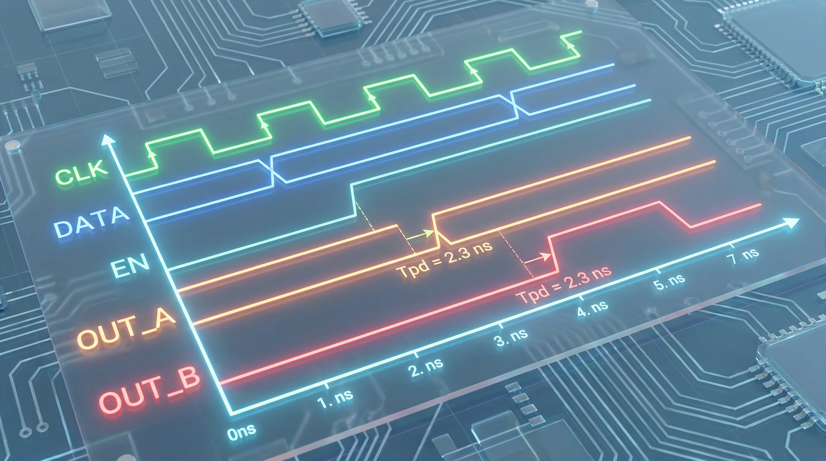
At its core, propagation delay, denoted as $t_{pd}$, is the finite time it takes for a logic gate's output to react to a change in its input. Think of it as a gate's reaction time. When an input signal flips, a complex chain reaction of physical events must occur before the output can follow suit.
This delay isn't a single, uniform value. We measure it in two distinct ways, because the underlying physics of switching a transistor 'on' versus 'off' are different:
- $t_{pLH}$ (Low-to-High Delay): The time taken for the output to transition from a logic 0 (low) to a logic 1 (high).
- $t_{pHL}$ (High-to-Low Delay): The time taken for the output to transition from a logic 1 (high) to a logic 0 (low).
In many modern CMOS circuits, the transistors responsible for pulling the output voltage up to '1' (PMOS) are inherently less efficient than the transistors that pull the output down to '0' (NMOS). This physical asymmetry often results in $t_{pLH}$ being slightly longer than $t_{pHL}$. For general analysis, engineers often use an average propagation delay, $t_{pd} = (t_{pLH} + t_{pHL}) / 2$, but for high-performance design, the distinction is critical.
The Physical Origins: Why Instant Is Impossible
Propagation delay isn't a flaw; it's a consequence of physics. Three primary factors contribute to this electronic inertia.
- Transistor Switching Time: At the heart of every logic gate are transistors, which act as microscopic, electrically-controlled switches. They don't flip instantly. Every transistor has a "gate," which acts like a small capacitor. To turn the transistor on, this capacitance must be charged; to turn it off, it must be discharged. This process is like filling or draining a tiny bucket—it requires a finite amount of current over a finite amount of time.
- Interconnect Capacitance: The metal wires, or "traces," that connect gates on a silicon die also possess capacitance. The longer the wire and the closer it is to other wires, the more capacitance it has. Every signal that travels down this wire must charge and discharge this capacitance, adding to the total delay. This is the "interconnect tax"—a performance penalty for every millimeter a signal must travel across the chip.
- Load Capacitance (Fan-Out): A single gate's output rarely drives just one other gate. It often connects to the inputs of several gates, a property known as "fan-out." Each of these inputs presents its own small capacitive load. The total delay is heavily influenced by the sum of all these loads. Imagine a single speaker trying to be heard by a crowd. The larger the crowd (the higher the fan-out), the more power is needed to ensure the message reaches everyone clearly and quickly.
The Critical Path: Your Circuit's Ultimate Speed Limit
In a simple circuit, the delay of a single gate might be negligible. But digital systems are composed of millions of gates arranged in complex chains. When gates are connected in series, their propagation delays add up.
This leads to one of the most important concepts in computer architecture: the critical path. The critical path is the longest-delay path through a combinational logic circuit, from an input (or a register output) to an output (or a register input). This path dictates the maximum operational speed of the entire circuit.
Consider the classic 4-bit ripple-carry adder. It's built from four full-adder circuits chained together. The sum bit for the first stage ($S_0$) is calculated quickly. However, the carry-out bit ($C_{out1}$) from this first stage is required to calculate the sum for the second stage ($S_1$). This dependency continues down the line. The final sum bit, $S_3$, cannot be calculated until the carry signal has "rippled" through all three preceding stages.
If each full adder has a carry-out propagation delay of $t_{pd_carry}$, the total delay to get a valid final carry bit is approximately $4 \times t_{pd_carry}$. For a 64-bit adder of this design, the delay would be $64 \times t_{pd_carry}$—an eternity in modern computing. This is precisely why more advanced architectures like carry-lookahead adders were invented: to break this linear chain of delay.
The critical path delay, $t_{pd(critical)}$, directly limits the maximum clock frequency ($f_{max}$) of a synchronous circuit. The clock period ($T_{clk}$) must be long enough for a signal to travel from one register, through the entire critical path of combinational logic, and arrive stably at the next register before the next clock edge arrives. This is governed by the setup time constraint:
$$T_{clk} \ge t_{clk-q} + t_{pd(critical)} + t_{setup}$$
Where:
- $t_{clk-q}$ is the time it takes for a register's output to change after a clock edge.
- $t_{pd(critical)}$ is the delay of the longest logic path between registers.
- $t_{setup}$ is the time the data must be stable at a register's input before the next clock edge.
The maximum clock frequency is therefore the inverse of this minimum period: $f_{max} = 1 / T_{clk(min)}$. Your multi-gigahertz CPU is, in essence, a testament to decades of engineering effort dedicated to minimizing every term in this equation.
The "Gotcha": Glitches, Hazards, and Race Conditions
When signals from a common source travel through different logic paths with unequal delays, they can arrive at their destination at different times. This phenomenon, known as a race condition, can give rise to temporary, unwanted pulses on a circuit's output called glitches or hazards.
Imagine a simple logic expression: $Y = A \cdot \overline{A}$. Mathematically, this should always be 0. Now, let's build it with real gates. The variable $A$ feeds directly into an AND gate. It also feeds into a NOT gate, whose output then goes to the same AND gate.
When $A$ transitions from 1 to 0, the direct path to the AND gate sees the '0' almost instantly. However, the other path must first go through the NOT gate, which introduces a propagation delay, $t_{pd(NOT)}$. For a brief moment—equal to $t_{pd(NOT)}$—both inputs to the AND gate will be '1' (the old value of A and the delayed, not-yet-updated output of the NOT gate). This causes the output $Y$ to glitch, momentarily pulsing to '1' when it should have remained at '0'.
While often harmless if the output is eventually sampled by a register after it has settled, in asynchronous systems or clock-gating logic, such glitches can cause catastrophic failures.
Simulating on digisim.io
Reading about nanosecond delays is one thing; seeing their effect is another. The digisim.io platform is the perfect laboratory for observing these phenomena firsthand.
A classic and visually compelling experiment is the ring oscillator.
- Build the Circuit: On the digisim.io canvas, place an odd number of NOT gates (inverters) in a chain. Three is a good starting point.
- Create the Loop: Connect the output of the last inverter back to the input of the first inverter.
- Observe the Oscillation: Attach a Logic Probe or an LED to any point in the loop. You will see it blinking!
What you've built is a circuit whose output is constantly chasing itself. The signal flips, propagates through the chain of inverters, and arrives back at the beginning, inverted, causing it to flip again. The time it takes to make one full oscillation is directly related to the cumulative propagation delay.
The period of oscillation will be approximately $T = 2 \times N \times t_{pd}$, where $N$ is the number of inverters and $t_{pd}$ is the average propagation delay of a single inverter. Head over to the Timing Diagram view in DigiSim to see a perfect square wave. Now, challenge yourself: add two more inverters to the chain (for a total of five). You will see the frequency of oscillation decrease, as the total propagation delay of the loop has increased. You are directly observing the impact of cumulative delay.
Real-World Use: Taming the Delay
Managing propagation delay is a daily battle for hardware engineers.
- CPU Core Design: The advertised clock speed of a processor is determined by the critical path within its most complex pipeline stage, often in the Arithmetic Logic Unit (ALU) or instruction scheduling logic. Engineers at companies like Intel and AMD use sophisticated Static Timing Analysis (STA) tools that automatically analyze every single path in a design (numbering in the billions) to find the critical one. They then use techniques like logic restructuring and transistor sizing to shorten it, squeezing out every last picosecond of performance.
- High-Speed Data Interfaces: Consider the DDR RAM in your computer. Data bits travel from the memory module to the CPU over parallel copper traces on the motherboard. If one bit's signal arrives later than another due to a longer trace (and thus greater propagation delay), the data becomes skewed and corrupted. To prevent this, motherboard designers meticulously route these traces in serpentine, snake-like patterns to ensure every single data line has the exact same physical length, and therefore, the same propagation delay.
Propagation delay is not an abstract nuisance. It is the physical heartbeat of digital computation. It dictates the tempo of our digital world, from the blink of an LED to the speed of a supercomputer. To design the future of hardware, we must first master this fundamental rhythm.
Ready to see this in action? Don't just take my word for it. Head over to digisim.io, build your own ring oscillator, and watch the physics of computation unfold before your eyes.