Propagation Delay: The Physics That Dictates Digital Speed
Propagation delay is the time a logic gate takes to react to an input change. It sets the critical path, max clock frequency, and circuit glitch behavior.

TL;DR: Propagation delay () is the finite time between a logic gate’s input changing and its output responding — typically a few nanoseconds. The longest such path through a circuit is the critical path, and it directly limits the maximum clock frequency: .
Propagation delay () is the finite time it takes for a logic gate’s output to respond to a change at its input. Real silicon switches in a few nanoseconds, not instantly. Across millions of chained gates inside a CPU, those nanoseconds add up to the critical path that sets the chip’s maximum clock frequency. Understanding propagation delay is the key to designing circuits that work outside a textbook.
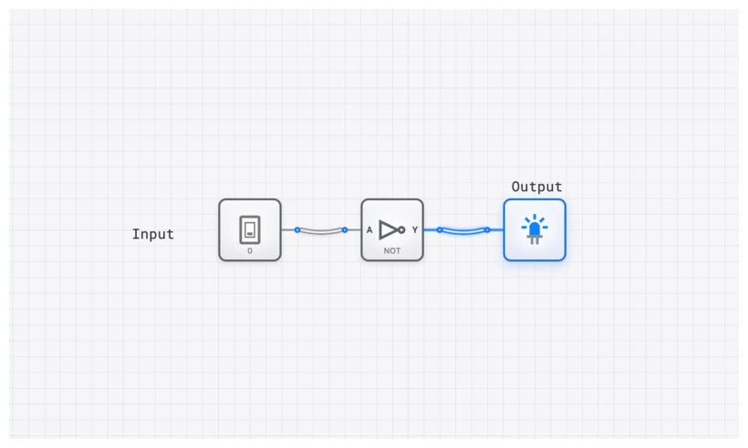
Explore the NOT Gate in digisim.io
The Anatomy of a Delay
At its core, propagation delay, denoted as , is the finite time it takes for a logic gate’s output to react to a change in its input. Think of it as a gate’s reaction time. When an input signal flips, a complex chain reaction of physical events must occur before the output can follow suit.
This delay isn’t a single, uniform value. We measure it in two distinct ways because the underlying physics of switching a transistor “on” versus “off” are different:
- (Low-to-High Delay): The time taken for the output to transition from a logic 0 (low) to a logic 1 (high).
- (High-to-Low Delay): The time taken for the output to transition from a logic 1 (high) to a logic 0 (low).
In many modern CMOS circuits, the transistors responsible for pulling the output voltage up to 1 (PMOS) are inherently less efficient than the transistors that pull the output down to 0 (NMOS). This physical asymmetry often results in being slightly longer than . For general analysis, engineers often use an average propagation delay:
For high-performance design, however, this distinction is critical. If you are designing a clock distribution network, even a few picoseconds of difference between these two values can lead to “duty cycle distortion,” where your clock is no longer a perfect 50/50 square wave.
Technical Specification: The NOT Gate
To understand delay, we must first understand the simplest logic element: the NOT gate. While its logic is trivial, its physical behavior is the foundation of all timing analysis.
| Input (A) | Output (Y) | Ideal Timing | Real-World Timing |
|---|---|---|---|
| 0 | 1 | Instant | Delayed by |
| 1 | 0 | Instant | Delayed by |
The Boolean expression for this operation is:
In a simulator like digisim.io, we often treat these gates as ideal for basic logic verification. But as you progress to timing-sensitive designs, you will find that ignoring these delays is the fastest way to build a circuit that works on paper but fails in silicon.
The Physical Origins: Why Instant is Impossible
Propagation delay isn’t a flaw; it’s a consequence of the universe we inhabit. Three primary factors contribute to this electronic inertia.
1. Transistor Switching Time
At the heart of every logic gate are transistors, which act as microscopic, electrically-controlled switches. They don’t flip instantly. Every transistor has a “gate” terminal that acts like a small capacitor. To turn the transistor on, this capacitance must be charged; to turn it off, it must be discharged. This process is like filling or draining a tiny bucket—it requires a finite amount of current over a finite amount of time.
2. Interconnect Capacitance
The metal wires, or “traces,” that connect gates on a silicon die also possess capacitance. The longer the wire and the closer it is to other wires, the more capacitance it has. Every signal that travels down this wire must charge and discharge this capacitance, adding to the total delay. This is the “interconnect tax”—a performance penalty for every millimeter a signal must travel across the chip.
3. Load Capacitance (Fan-Out)
A single gate’s output rarely drives just one other gate. It often connects to the inputs of several gates, a property known as “fan-out.” Each of these inputs presents its own small capacitive load. The total delay is heavily influenced by the sum of all these loads. Imagine a single speaker trying to be heard by a crowd. The larger the crowd (the higher the fan-out), the more power is needed to ensure the message reaches everyone clearly and quickly.
The Critical Path: Your Circuit’s Ultimate Speed Limit
In a simple circuit, the delay of a single gate might be negligible. But digital systems are composed of millions of gates arranged in complex chains. When gates are connected in series, their propagation delays add up.
This leads to one of the most important concepts in computer architecture: the Critical Path. The critical path is the longest-delay path through a combinational logic circuit, from an input (or a register output) to an output (or a register input). This path dictates the maximum operational speed of the entire circuit.
Consider the classic 4-bit ripple-carry adder, which you can build using the ADDER component in digisim.io. It’s built from four full-adder circuits chained together. The sum bit for the first stage () is calculated quickly. However, the carry-out bit () from this first stage is required to calculate the sum for the second stage (). This dependency continues down the line. The final sum bit, , cannot be calculated until the carry signal has “rippled” through all three preceding stages.
If each full adder has a carry-out propagation delay of , the total delay to get a valid final carry bit is approximately . For a 64-bit adder of this design, the delay would be —an eternity in modern computing. This is precisely why more advanced architectures like carry-lookahead adders were invented: to break this linear chain of delay.
The critical path delay, , directly limits the maximum clock frequency () of a synchronous circuit. The clock period () must be long enough for a signal to travel from one REGISTER, through the entire critical path of combinational logic, and arrive stably at the next REGISTER before the next clock edge arrives. This is governed by the setup time constraint:
Where:
- is the time it takes for a register’s output to change after a clock edge.
- is the delay of the longest logic path between registers.
- is the time the data must be stable at a register’s input before the next clock edge.
The maximum clock frequency is therefore the inverse of this minimum period:
Your multi-gigahertz CPU is, in essence, a testament to decades of engineering effort dedicated to minimizing every term in this equation.
Analyze a 4-Bit Counter’s Timing
Common Pitfall: Glitches, Hazards, and Race Conditions
When signals from a common source travel through different logic paths with unequal delays, they can arrive at their destination at different times. This race condition can give rise to temporary, unwanted pulses on a circuit’s output called glitches or hazards.
A common example: . Mathematically this is always 0. Built from real gates, feeds directly into an AND gate, and also feeds into a NOT gate whose output goes to the same AND gate.
When transitions from 0 to 1, the direct path to the AND gate sees the new 1 almost instantly. However, the other path must first go through the NOT gate, which introduces a propagation delay, . For a brief moment — equal to — both inputs to the AND gate will be 1 (the new value of on the direct path, and the old value of still propagating through the inverter). This causes the output to glitch, momentarily pulsing to 1 when it should have remained at 0. (Textbooks call this a static-0 hazard: the output is supposed to stay LOW but briefly goes HIGH.)
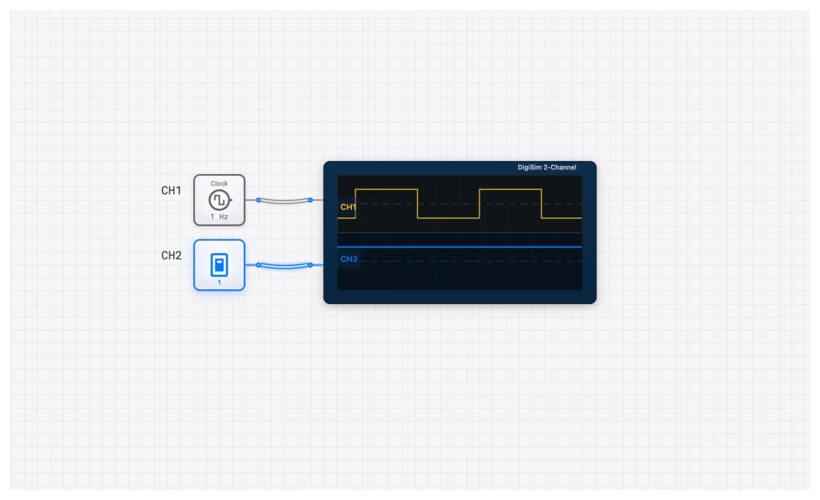
While often harmless if the output is eventually sampled by a REGISTER after it has settled, in asynchronous systems or clock-gating logic, such glitches can cause catastrophic failures. This is why we use the OSCILLOSCOPE in digisim.io to hunt for these “spikes” in the waveform.
Visualizing Delay with the Ring Oscillator
Reading about nanosecond delays is one thing; seeing their effect is another. The digisim.io platform is the perfect laboratory for observing these phenomena firsthand. A classic and visually compelling experiment is the Ring Oscillator.
A ring oscillator is a device composed of an odd number of NOT gates whose output is fed back into the input. Because there is no stable state, the circuit oscillates. The frequency of this oscillation is entirely dependent on the propagation delay of the gates.
Step-by-Step Build:
- Place the Gates: On the digisim.io canvas, place three NOT gates in a row.
- Chain Them: Connect the output of the first to the input of the second, and the second to the third.
- Close the Loop: Connect the output of the third NOT gate back to the input of the first.
- Add Instrumentation: Connect an OSCILLOSCOPE to the output of the third gate.
What you’ve built is a circuit whose output is constantly chasing itself. The signal flips, propagates through the chain of inverters, and arrives back at the beginning, inverted, causing it to flip again. The time it takes to make one full oscillation is directly related to the cumulative propagation delay.
The period of oscillation will be approximately:
where is the number of inverters and is the average propagation delay of a single inverter. The factor of 2 appears because a complete oscillation requires the signal to traverse the chain twice: once to transition HIGH and once to transition LOW. The oscillation frequency is therefore:
If you add two more NOT gates to the chain (for a total of five), you will see the frequency of oscillation decrease. You are directly observing the impact of cumulative delay. By measuring the frequency with an OSCILLOSCOPE and knowing , you can solve for of a single gate, which is exactly how chip manufacturers characterize their fabrication processes.
Real-World Use: Taming the Delay
Managing propagation delay is a daily battle for hardware engineers. It isn’t just about making things faster; it’s about making them work at all.
CPU Core Design
The advertised clock speed of a processor is determined by the critical path within its most complex pipeline stage, often in the ALU_8BIT or instruction scheduling logic. Engineers at companies like Intel and AMD use sophisticated Static Timing Analysis (STA) tools that automatically analyze every single path in a design (numbering in the billions) to find the critical one. They then use techniques like logic restructuring and transistor sizing to shorten it, squeezing out every last picosecond of performance.
High-Speed Data Interfaces
Consider the DDR5 RAM in a modern workstation. Data bits travel from the memory module to the CPU over parallel copper traces on the motherboard. If one bit’s signal arrives later than another due to a longer trace (and thus greater propagation delay), the data becomes skewed and corrupted. To prevent this, motherboard designers meticulously route these traces in serpentine, snake-like patterns to ensure every single data line has the exact same physical length, and therefore, the same propagation delay. This is known as “length matching.”
Mastering the Rhythm of Logic
Propagation delay is not an abstract nuisance. It is the physical heartbeat of digital computation. It dictates the tempo of our digital world, from the blink of an OUTPUT_LIGHT to the speed of a supercomputer. To design the future of hardware, we must first master this fundamental rhythm.
Keep the OSCILLOSCOPE open as you work through the digisim.io curriculum. The slight lag between a CLOCK edge and a REGISTER output is not a simulation bug — it is the simulation of reality.
Continue with setup, hold, and metastability for the timing constraints that flow from propagation delay, or multi-input logic gates for cascade-vs-tree delay analysis. Open the NOT gate component reference and try the ring-oscillator build above.