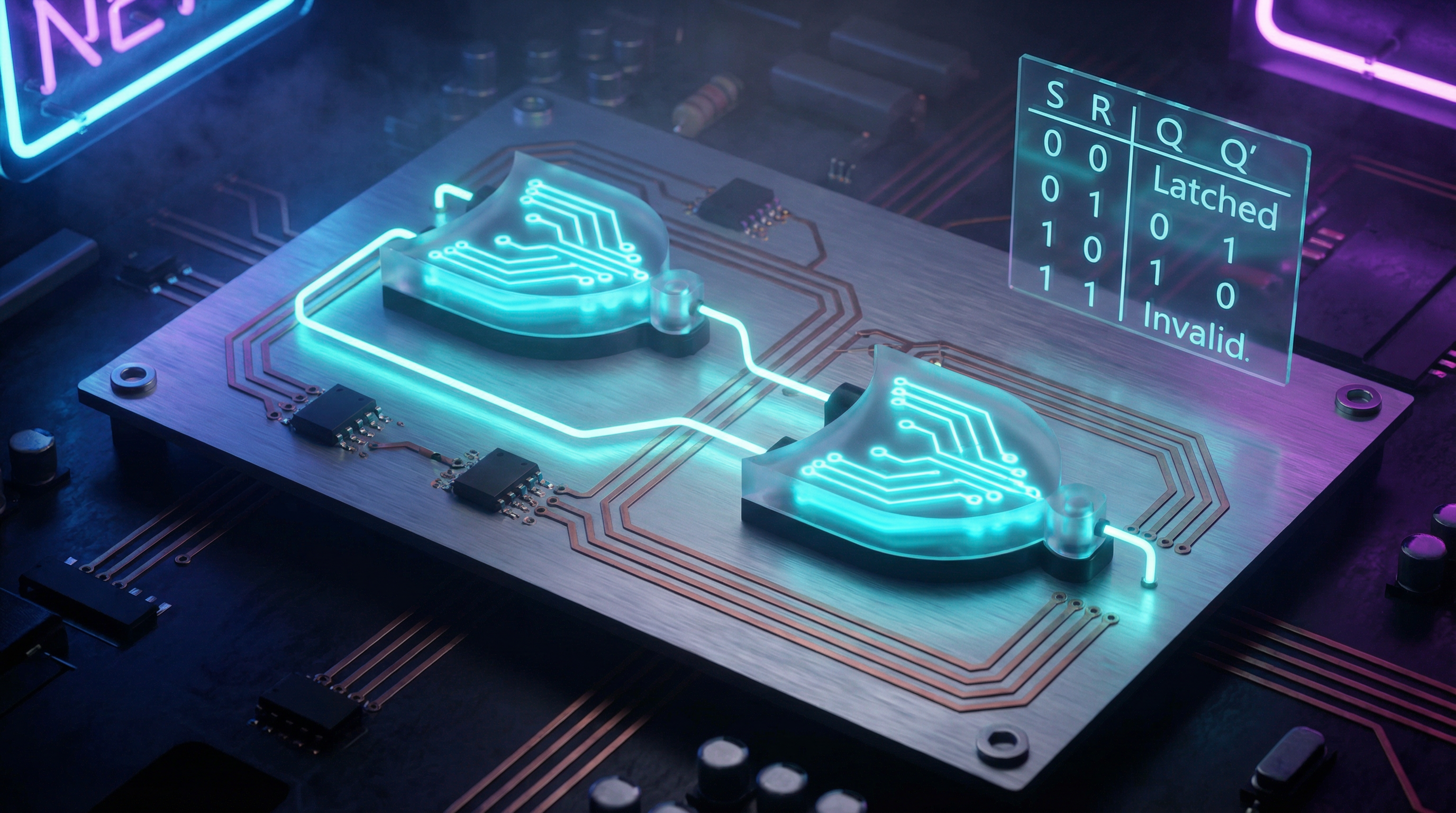
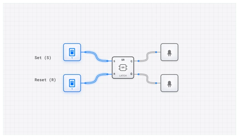
The SR Latch gave us the gift of memory—the ability for a circuit to hold state. But it came with a serious flaw: the forbidden state. Apply S=1 and R=1 simultaneously, and the circuit’s output becomes unpredictable. For decades, this limitation forced engineers to carefully constrain their designs, always guarding against the possibility that two independent control signals might collide.
The D Latch is the engineering solution to that problem. It is not merely a different circuit—it is a redesign of the SR Latch that makes the forbidden state physically impossible. Understanding how and why this transformation works is essential for anyone learning digital design, because it demonstrates a pattern you will see again and again: identifying a flaw in an existing design and solving it with structural constraints rather than behavioral rules.
The Problem: Why the SR Latch Needed Fixing
To appreciate the D Latch, you first need to feel the pain it solves. Recall the SR Latch truth table:
| S | R | Action | |
|---|---|---|---|
| 0 | 0 | Q | Hold |
| 0 | 1 | 0 | Reset |
| 1 | 0 | 1 | Set |
| 1 | 1 | ? | Forbidden |
The S and R inputs are independent. Nothing in the circuit prevents them from being ‘1’ at the same time. In a simple system with manual switches, you can just tell users “don’t press both buttons.” But in a complex digital system where S and R are driven by other logic, glitches and propagation delays can momentarily assert both signals. The forbidden state is not just a theoretical concern—it is a reliability hazard.
Engineers needed a structural guarantee: a circuit where the forbidden condition cannot occur by construction, not merely by convention.
The Solution: From Two Inputs to One
The D Latch’s core insight is deceptively simple: replace the two independent inputs (S and R) with a single data input (D), and derive S and R internally so they are always complementary.
Here is the transformation, step by step:
Step 1: Start with a Gated SR Latch
First, add an Enable signal to the SR Latch. Place an AND gate on each input:
When Enable is low, both internal S and R are forced to ‘0’, putting the SR core into Hold mode regardless of the external inputs. This gives us controlled data capture—the latch only “listens” when enabled.
Step 2: Eliminate the Second Input
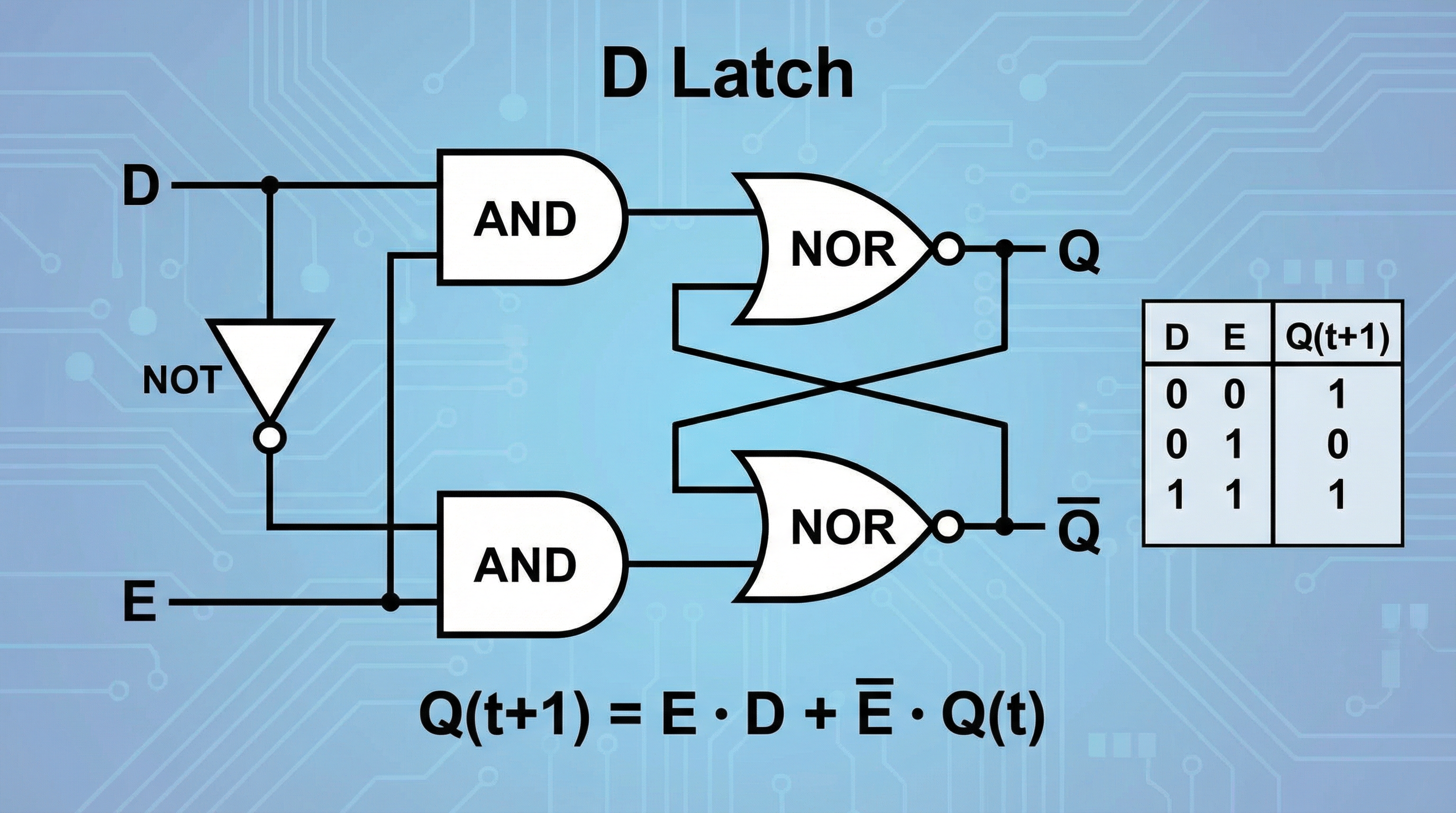
Now comes the critical modification. Instead of having separate S and R inputs, use a single D (Data) input and a NOT gate:
Since D and are always complements, and can never both be ‘1’ at the same time. The forbidden state is eliminated by construction.
The Circuit Transformation Visualized
Here is the progression from SR Latch to D Latch in terms of gate-level structure:
SR Latch: Two cross-coupled NOR gates. Two independent inputs.
Gated SR Latch: Two cross-coupled NOR gates + two AND gates for enable control. Three independent inputs (S, R, E). Forbidden state still possible when E=1, S=1, R=1.
D Latch: Two cross-coupled NOR gates + two AND gates + one NOT gate. Two independent inputs (D, E). Forbidden state eliminated.
The NOT gate is the key. One gate, costing practically nothing in silicon area, transforms an unreliable circuit into a dependable one.
SR Latch vs. D Latch: A Direct Comparison
| Property | SR Latch | D Latch |
|---|---|---|
| Data inputs | 2 (S, R) | 1 (D) |
| Control input | None (basic) or Enable (gated) | Enable (E) |
| Forbidden state | S=1, R=1 causes invalid output | Impossible by construction |
| Set operation | S=1, R=0 | E=1, D=1 |
| Reset operation | S=0, R=1 | E=1, D=0 |
| Hold operation | S=0, R=0 | E=0 |
| Transparency | Always transparent (basic) | Transparent only when E=1 |
| Characteristic equation | (constraint: ) |
The D Latch trades flexibility for safety. You lose the ability to independently control Set and Reset, but you gain a circuit that is inherently well-behaved.
The Truth Table and Characteristic Equation
| E (Enable) | D (Data) | Action | |
|---|---|---|---|
| 0 | X | Hold (Latched) | |
| 1 | 0 | 0 | Reset (Transparent) |
| 1 | 1 | 1 | Set (Transparent) |
The characteristic equation:
Read this as a conditional: “If enabled, capture D. If not enabled, hold Q.” The equation is functionally a 2-to-1 multiplexer, with the Enable signal selecting between new data and the stored value.
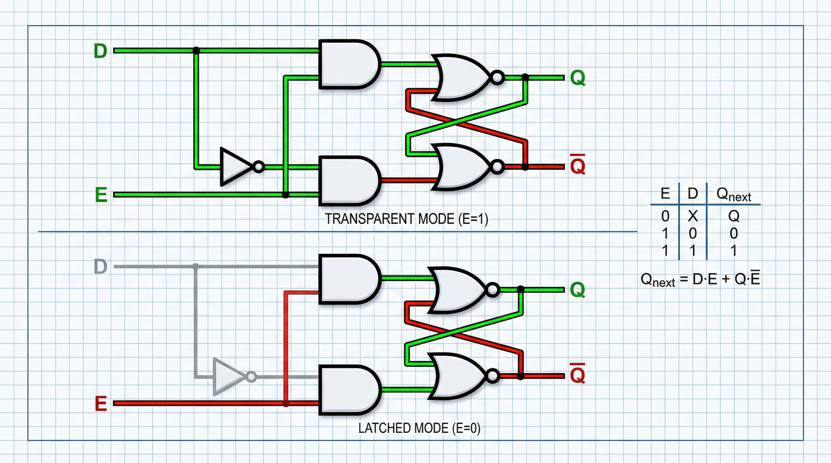
What Transparency Means (and Why It Matters)
The D Latch operates in two modes:
- Transparent mode (): Q follows D in real time. Every change on D immediately appears on Q.
- Latched mode (): Q holds its last value. D is ignored.
This level-sensitive behavior is both the D Latch’s utility and its limitation. While the enable window is open, glitches on the D line pass straight through to the output. In fast synchronous systems, this transparency can cause unintended state changes. This vulnerability is exactly what motivates the next step in the evolution: the edge-triggered D Flip-Flop, which narrows the capture window to a single clock transition.
Oscilloscope Verification
On digisim.io, you can observe transparency directly using the OSCILLOSCOPE. Connect E to Channel 1, D to Channel 2, and Q to Channel 3. While E is high, the D and Q waveforms will be identical. The moment E drops low, the Q waveform freezes into a flat line regardless of what D does.
Real-World Applications
1. Address Demultiplexing (The Intel 8086 Legacy)
Early microprocessors like the Intel 8085 and 8086 shared pins between address and data signals to reduce chip package size. An external D Latch (the 74LS373 Octal Transparent Latch) captured the address portion when the processor pulsed ALE (Address Latch Enable) high. Once ALE dropped low, the latch held the address steady while the same pins switched to carrying data.
2. Pipeline Registers
In pipelined CPU architectures, banks of latches between pipeline stages (Fetch, Decode, Execute) hold intermediate results steady so each stage can operate on stable data while the preceding stage processes the next instruction.
Building the D Latch from Gates
Building the circuit from discrete gates makes the SR-to-D transformation tangible.
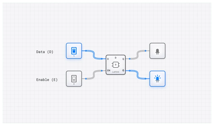
- Place two INPUT_SWITCH components. Label one
Dataand the otherEnable. - Build the steering logic. Place two AND gates and one NOT gate. Connect
Datato the first AND gate and to the NOT gate. Connect the NOT gate output to the second AND gate. ConnectEnableto both AND gates. - Build the memory core. Place two cross-coupled NOR gates. Connect the first AND gate output to one NOR gate, and the second AND gate output to the other.
- Close the feedback loop. Connect each NOR gate’s output to an input of the other NOR gate.
- Add output. Connect an OUTPUT_LIGHT to the Q output.
Toggle Enable to ‘1’, then flip Data back and forth—the output follows instantly. Toggle Enable to ‘0’, and the output freezes. You have built a one-bit memory cell with no forbidden state.
The Evolutionary Chain
The D Latch is one link in a clear progression of increasingly robust memory elements:
- SR Latch — Memory with a forbidden state.
- D Latch — Memory without a forbidden state, but with transparency.
- D Flip-Flop — Memory without transparency, capturing data only at clock edges.
- Registers — Arrays of flip-flops storing multi-bit values.
Each step solves a specific problem introduced by the previous design. Understanding this evolution—not just memorizing each circuit in isolation—is what separates a student who can draw schematics from an engineer who can design reliable systems.
Ready to build? The simulator is open.