Ever wonder how your computer actually “holds” a number? When you’re adding two values in a CPU, those numbers don’t just float in the ether; they are physically locked into place by a fundamental circuit called a register. If the logic gate is the atom of computing, the register is the first molecule of memory.
A register is essentially a group of flip-flops—usually the D_FLIP_FLOP variety—working in perfect synchronization to store multiple bits of data simultaneously. In this guide, we’re focusing on the 4-bit register, the classic “nibble” storage unit that serves as the backbone for everything from program counters to accumulator registers in early microprocessors like the MOS 6502 or the Intel 8008.
What Exactly is a Register?
In the hierarchy of digital systems, a register sits right above the individual latch. While a single D_LATCH or D_FLIP_FLOP can remember one bit, a register scales this up. A 4-bit register captures four bits of data (D3, D2, D1, D0) at the exact moment a CLOCK signal transitions from LOW to HIGH.
The beauty of the register is its “parallel” nature. Unlike serial communication where bits trickle in one by one, a register grabs the entire 4-bit value at once. It’s the difference between a single person walking through a door and a row of four people stepping through a gate in unison.
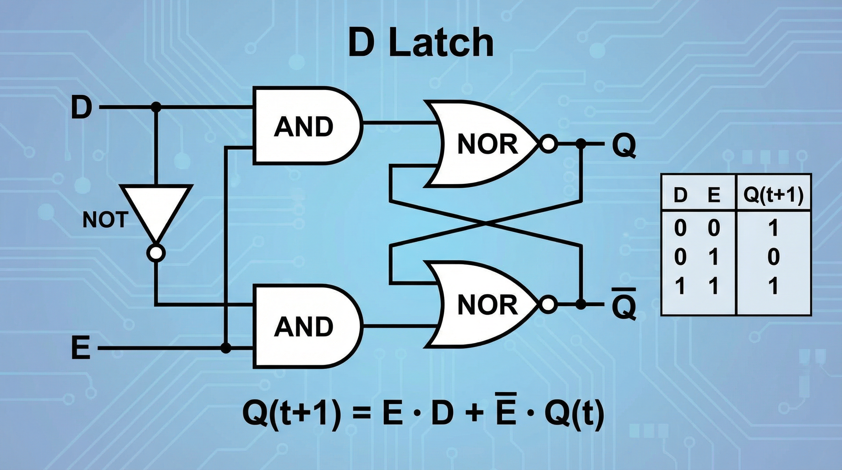
Technical Specification & Truth Table
The behavior of a 4-bit register is governed by the edge-triggered nature of its internal components. In digisim.io, we typically use the D_FLIP_FLOP because it prevents the “transparency” issues found in basic latches.
Here is the truth table for a single bit within the register. Multiply this by four, and you have your 4-bit storage:
| CLOCK | D (Input) | Q (Current) | Q_next (After Edge) | State |
|---|---|---|---|---|
| 0 | X | 0 | 0 | Hold |
| 1 | X | 1 | 1 | Hold |
| ↑ (Rising) | 0 | X | 0 | Load 0 |
| ↑ (Rising) | 1 | X | 1 | Load 1 |
| ↓ (Falling) | X | Q | Q | Hold |
In this table, represents a “don’t care” state, and represents the rising edge of the CLOCK.
The Mathematical Foundation
The logic of a standard D_FLIP_FLOP is the simplest in the sequential world. The characteristic equation is:
However, a professional-grade register rarely just “loads” on every single clock tick. We usually want a “Load Enable” feature. When we add a MULTIPLEXER to the input of each flip-flop, the equation evolves into a conditional storage formula:
This formula tells us that if is 1, we take the new data . If is 0, we feed the current output back into the input, effectively “holding” the value regardless of what the clock is doing.
Common Pitfall: Why Your Register Might Be Glitching
I’ve seen countless students build a register and wonder why the data looks like “garbage” on the output. The culprit is almost always Setup and Hold Times.
In a simulator like digisim.io, propagation delay is modeled to reflect real-world physics. If your data input changes at the exact same picosecond as the CLOCK rising edge, the flip-flop enters a state of “metastability.” It doesn’t know if it should be a 0 or a 1.
The Rule: Data must be stable for a duration of before the clock edge and remain stable for after the edge. If you’re toggling an INPUT_SWITCH manually while a high-speed CLOCK is running, you’re bound to hit a race condition.
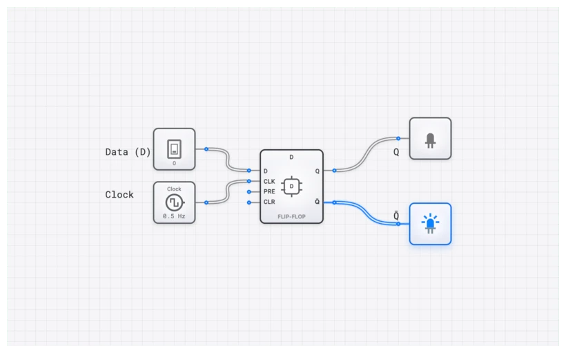
Interactive Demo: Building the Foundation
Before we get into complex CPU registers, you need to see how a single bit behaves under pressure. I recommend starting with the basic edge-triggered D-type circuit to understand the “shutter” effect of the clock.
Why this circuit? It isolates the timing. You can toggle the input and see that the output only updates when you manually pulse the clock. This is the “Aha!” moment for most students.
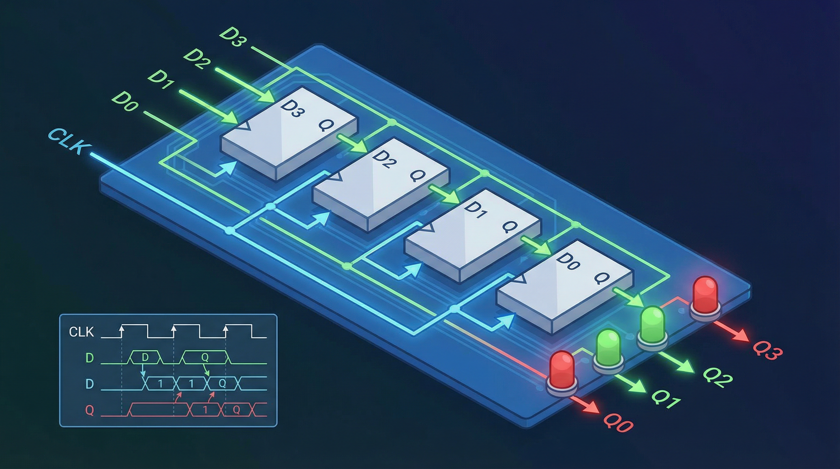
Scaling Up: The 4-Bit Register with Load Enable
Once you have mastered the single bit, it is time to build the 4-bit version. In a real system, we rarely want the register to capture new data on every single clock edge. Instead, we need a Load Enable signal that controls when the register accepts new data and when it holds its current value.
How Load Enable Works
The Load Enable mechanism places a 2-to-1 multiplexer in front of each flip-flop’s D input:
- When : The multiplexer selects the external data input (), and the flip-flop captures the new value on the next clock edge.
- When : The multiplexer feeds the flip-flop’s own Q output back to its D input, so the flip-flop recaptures its current value on each clock edge—effectively holding state.
This corresponds to the conditional equation we derived earlier:
The clock still runs continuously, but the register only updates its stored value when Load is asserted. This is critical in CPU design: the clock ticks every cycle, but a register like the accumulator should only load a new result when the control unit commands it.
Parallel Load Operation
All four flip-flops share the same clock line, so when Load is asserted and the clock edge arrives, all four bits are captured simultaneously. This is parallel load—the entire 4-bit value is stored in a single clock cycle, as opposed to serial load (used in shift registers) where bits enter one at a time over four cycles.
Parallel load ensures data integrity: you never have a “half-updated” register where some bits reflect the new value and others still hold the old one. Every bit transitions together at the same clock edge.
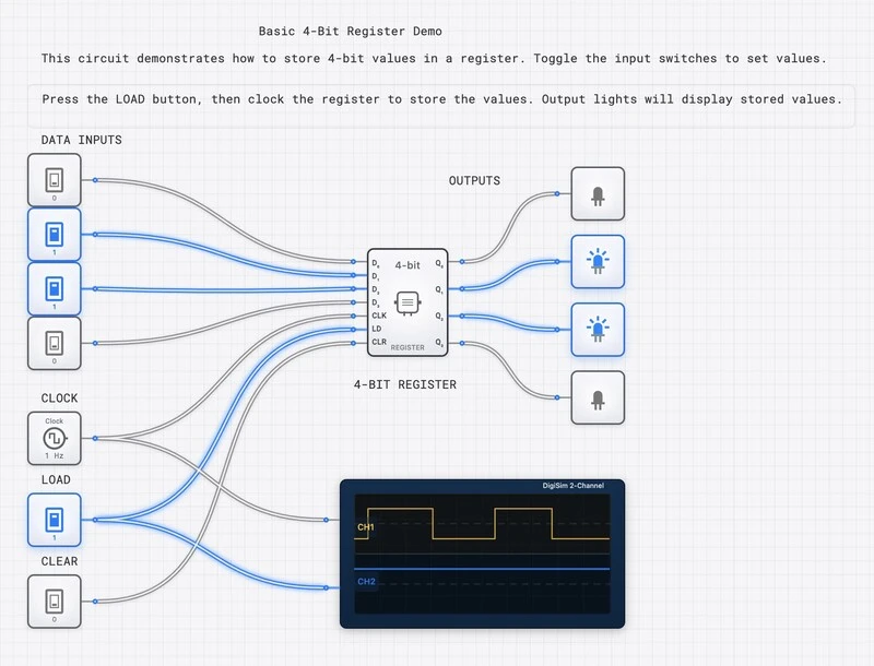
Oscilloscope Verification: Seeing the “Snapshots”
To truly understand a register, you need to stop looking at static lights and start looking at time. Use the OSCILLOSCOPE_8CH in digisim.io to monitor the CLOCK, the four inputs, and the four outputs.
- Connect Channel 0 to your CLOCK.
- Connect Channels 1-4 to your outputs (Q3-Q0).
- Run the simulation and change the input values.
- Observe how the output waveforms are “flat” until the exact moment the clock signal spikes.
This visual representation proves that the register is a “sampling” device. It ignores the chaos of the data bus and only listens to the values at the precise moment of the clock’s command.
Real-World Applications
You cannot build a computer without registers. They are the “scratchpad” of the processor.
- The Intel 8086 Accumulator (AX): This is a 16-bit register (essentially four 4-bit registers chained together). When you perform an instruction like
ADD AX, BX, the result is latched into the AX register at the end of the execution cycle. - Instruction Registers (IR): In almost every CPU architecture, the INSTRUCTION_REGISTER holds the current opcode being executed. Without this, the CPU would “forget” what it was doing halfway through a clock cycle as the memory bus changed.
- Pipeline Stages: Modern processors use registers to separate different stages of execution (Fetch, Decode, Execute). These are called “Pipeline Registers,” and they allow the CPU to work on multiple instructions at once without them bleeding into each other.
Your Next Step: From Storage to Movement
Now that you’ve built a circuit that can hold a nibble, the next logical question is: how do we move that data around? In a CPU, data doesn’t just sit in one register; it flows from the ALU to the ACCUMULATOR, and then out to RAM.
Try adding a TRI_STATE_BUFFER_8BIT to your register output. This will allow you to connect multiple registers to a single DATA_BUS_8BIT without causing a short circuit. It’s the first step toward building your own functional CPU.