Mastering Shift Registers: From Serial to Parallel Conversion
Shift registers chain D flip-flops to move data one bit per clock pulse. Build SIPO, PISO, and PIPO variants and learn how UART and LED matrix drivers use them.

TL;DR: A shift register is a chain of D flip-flops where the output of each stage feeds the input of the next. On every clock edge, every bit shifts one position. Configurations are SISO, SIPO (serial-to-parallel — used by 74HC595 LED drivers), PISO (parallel-to-serial — used by UART transmitters), and PIPO.
A shift register moves data through hardware one bit per clock cycle. It is the bridge between the serial world (bits travel one by one over a single wire) and the parallel world (bits move in groups across a bus). The same primitive sits inside UART transmitters, LED-matrix drivers, and the bit-shifting unit of every ALU.
What Exactly is a Shift Register?
At its core, a shift register is a synchronous sequential circuit. It consists of a chain of flip-flops—typically the D_FLIP_FLOP—connected in a “bucket brigade” fashion. Each stage in the chain stores exactly one bit of data. When a clock pulse arrives, every bit in the register moves one position to the right (or left), like commuters moving up one seat on a train.
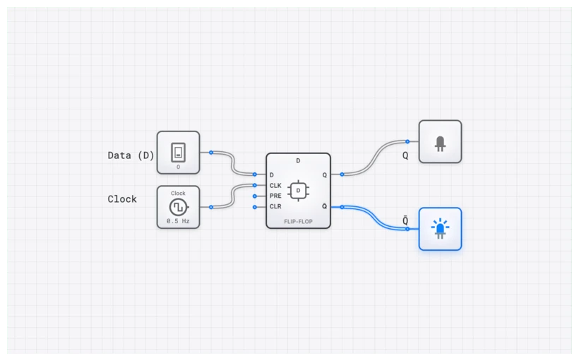
The digisim.io SHIFT_REGISTER component abstracts this complexity, but the propagation is most visible when you build one from individual D_FLIP_FLOP units.
Explore the D_FLIP_FLOP Component
The Mathematical Foundation
The behavior of a single stage in a shift register is governed by the characteristic equation of the D_FLIP_FLOP:
In a multi-stage shift register, the input of the -th stage is connected to the output of the -th stage. Therefore, the state of the entire register at time can be described as:
This simple relationship is what allows data to “flow” through the hardware.
The Four Flavors of Data Movement
Not all shift registers are created equal. Depending on how data enters and how it exits, we categorize them into four primary types. Understanding these distinctions is essential for choosing the right configuration for any given application.
1. SISO: Serial-In, Serial-Out
Input: One bit per clock cycle. Output: One bit per clock cycle, delayed.
The SISO is the simplest form. Data enters one bit at a time and exits one bit at a time from the opposite end. It functions as a digital delay line: if you have a 4-bit SISO register, a bit entering now will not appear at the output until four clock cycles later. This makes SISO registers useful for signal timing adjustments and synchronization buffers.
2. SIPO: Serial-In, Parallel-Out
Input: One bit per clock cycle. Output: All bits available simultaneously.
The SIPO is the “expansion” configuration. You feed it a serial stream of bits, and once the register is full, you read all the outputs () simultaneously. This is exactly how we drive large LED matrices or LCD screens using very few pins on a microcontroller. The 74HC595 IC, discussed below, is a classic SIPO register.
3. PISO: Parallel-In, Serial-Out
Input: All bits loaded simultaneously. Output: One bit per clock cycle.
The PISO does the reverse of the SIPO. It takes a whole “word” of data (like 8 bits from a DATA_BUS_8BIT) and serializes it into a stream of individual bits. This is the heart of every UART (Universal Asynchronous Receiver-Transmitter) transmitter: the CPU loads a byte in parallel, and the PISO shifts it out one bit at a time over the serial line.
4. PIPO: Parallel-In, Parallel-Out
Input: All bits loaded simultaneously. Output: All bits available simultaneously.
A PIPO can load data in parallel and output it in parallel. On its own, this behaves like a standard REGISTER—useful for latching data at a clock edge. However, a “Universal” shift register combines PIPO with shifting capability, allowing it to operate in any of the four modes via control signals. This versatility makes it indispensable for arithmetic operations like bit-shifting for multiplication ( = multiply by 2) and division ( = divide by 2).

The Technical Specification: A 4-Bit SIPO Truth Table
Let’s look at how a 4-bit SIPO (Serial-In, Parallel-Out) behaves over four clock cycles. Assume we are shifting in the binary sequence (starting with the rightmost bit).
| Clock Pulse | Serial Input () | ||||
|---|---|---|---|---|---|
| Initial | 0 | 0 | 0 | 0 | 0 |
| 1 | 1 | 0 | 0 | 0 | |
| 1 | 1 | 1 | 0 | 0 | |
| 0 | 0 | 1 | 1 | 0 | |
| 1 | 1 | 0 | 1 | 1 |
Notice how the “1” that entered at moved from to to and finally to . This is the “shift” in action.
Common Pitfall: Timing and Propagation Delays
Race conditions are the most common shift-register bug. Timing matters because all flip-flops respond to the same clock edge.
Because all flip-flops share the same CLOCK signal, they all try to change state at the exact same moment. For this to work, the output of Stage A must remain stable long enough for Stage B to “grab” it. This involves three critical parameters:
- Setup Time (): The minimum time the data must be stable before the clock edge.
- Hold Time (): The minimum time the data must remain stable after the clock edge.
- Propagation Delay (): The time it takes for the output to change after the clock edge.
If your is shorter than your , the second flip-flop might grab the new value instead of the old one, causing the data to skip a stage or become corrupted. See setup, hold, and metastability for the full timing analysis. If you’re seeing glitches, pull out the OSCILLOSCOPE_8CH.
Verifying Behavior with the OSCILLOSCOPE_8CH
When you’re building a SHIFT_REGISTER_8BIT, looking at the OUTPUT_LIGHT components isn’t enough—they blink too fast for the human eye to track at high clock speeds.
To truly verify your circuit:
- Connect the CLOCK to Channel 1 of the OSCILLOSCOPE_8CH.
- Connect the Serial Input to Channel 2.
- Connect the parallel outputs ( through ) to the remaining channels.
When you run the simulation, you’ll see a beautiful “staircase” pattern. You’ll see the pulse on the Serial Input line appear on after the first clock edge, then on after the second, and so on. If the pulses don’t align perfectly with the rising edges of the clock, you’ve found your timing bug.
Real-World Applications: From 1978 to Today
Shift registers aren’t just academic exercises; they are the workhorses of the electronics industry.
1. The 74HC595 and LED Control
If you’ve ever used an Arduino, you’ve likely encountered the 74HC595. It’s an 8-bit SIPO shift register with a built-in latch. It allows you to control 8 LEDs using only 3 pins. By cascading (daisy-chaining) these chips, you can control hundreds of LEDs. We cover this extensively in our curriculum on digisim.io.
2. UART in the Intel 8086
In early computing, the Intel 8086 used shift registers to handle serial communication. To send a byte over a wire, the CPU would load the byte into a PISO shift register and clock it out bit-by-bit. On the receiving end, a SIPO register would collect the bits and present the full byte back to the receiving CPU.
3. Multiplication and Division
Did you know that shifting a binary number one position to the left is mathematically equivalent to multiplying it by 2?
Modern ALUs (Arithmetic Logic Units) use high-speed shift registers to perform these operations in a single clock cycle.
Building Your First Shift Register on digisim.io
Ready to get your hands dirty? Follow these steps to build a 4-bit SIPO register:
- Place the Stages: Drop four D_FLIP_FLOP components onto the canvas.
- Chain the Data: Connect the output of the first flip-flop to the input of the second. Repeat for all stages.
- Common Clock: Place a CLOCK component and connect it to the clock input of all four flip-flops. This is vital—they must be synchronous.
- Input and Output: Connect an INPUT_SWITCH to the input of the first flip-flop. Connect an OUTPUT_LIGHT to each output.
- The SimCast Advantage: Use the SimCast feature to record your circuit’s behavior. Toggle the input switch, pulse the clock, and watch the “1” move through the lights.
Final Thoughts
The shift register is the ultimate proof that complex behavior can emerge from simple parts. By just chaining a few flip-flops together, we gain the ability to convert data formats, delay signals, and perform math.
Try building a 4-bit bidirectional shift register that can shift both left and right based on a control switch — combining a SHIFT_REGISTER with a multiplexer on each stage’s data input.
Continue with the 4-bit register to see parallel-load storage, or open the D_FLIP_FLOP component reference — the storage element behind every shift-register stage.