De Morgan's Laws in Practice: NAND-Only Circuit Design
De Morgan's Laws convert NAND to bubbled-OR and NOR to bubbled-AND. Apply them to build NAND-only or NOR-only circuits and optimize multi-level logic.

TL;DR: De Morgan’s two identities — and — let you swap AND for OR (and vice versa) by distributing inversion. The practical payoff: any logic function can be implemented in NAND-only or NOR-only form, which is exactly what CMOS chip designers and FPGA synthesizers do.
The two De Morgan identities — and — are easy to memorize. The harder question is how working engineers actually use them. The answer spans CMOS transistor-level design, FPGA synthesis, NAND-only and NOR-only implementations, and multi-level circuit optimization.
This article focuses on putting De Morgan’s Laws to work in real design scenarios — how they shrink gate counts in actual circuits, how they let you implement any logic in NAND-only or NOR-only form, and how the simulator makes the equivalences obvious.
Quick Recap: The Two Laws
For reference, De Morgan’s two identities:
These generalize to variables:
Application 1: Converting to NAND-Only Implementation
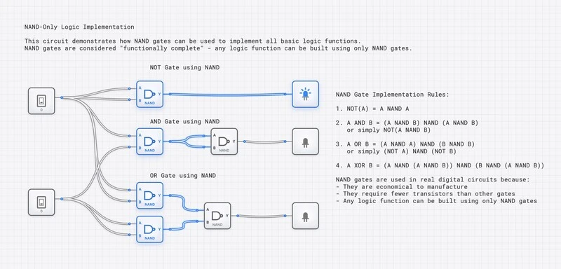
In CMOS technology, NAND gates are physically smaller and faster than AND or OR gates. A standard AND gate in CMOS is actually a NAND followed by an inverter — it already uses more transistors. For this reason, ASIC and FPGA designers routinely convert entire circuits to use only NAND gates.
The Conversion Process
Any Sum-of-Products (SOP) expression can be converted to NAND-NAND form in two steps:
- Start with the SOP:
- Apply double negation:
- Apply De Morgan’s to the outer bar:
The result is a two-level NAND-NAND circuit: the first level NANDs compute and , and the second level NAND combines them.
Worked Example: 3-Variable Function
Convert to NAND-only:
Step 1: Double-negate:
Step 2: Apply De Morgan’s to the outer bar:
Implementation:
- Gate 1 (NAND): Inputs , , — outputs
- Gate 2 (NAND): Inputs , , — outputs
- Gate 3 (NAND): Inputs are outputs of Gate 1 and Gate 2 — outputs
The NOT gates for and are themselves implemented as single-input NANDs (tie both inputs together).
Gate count: 3 NAND gates + 2 inverters (single-input NANDs) = 5 identical gates. Compare this to the AND-OR version, which requires 2 AND gates, 1 OR gate, and 2 NOT gates — five gates of three different types. The NAND-only version uses a single gate type, simplifying manufacturing and reducing the variety of cells needed on silicon.
Try NAND Universal Logic Template
Application 2: Converting to NOR-Only Implementation
The dual of the NAND-NAND conversion works for Product-of-Sums (POS) expressions, yielding NOR-NOR circuits.
The Conversion Process
- Start with a POS:
- Double-negate:
- Apply De Morgan’s to the outer bar:
The result is a two-level NOR-NOR circuit: the first level NORs compute and , and the second NOR combines them.
In CMOS processes optimized for PMOS transistors (such as some low-power designs), NOR gates can be preferred over NAND gates. The choice between NAND-only and NOR-only depends on the specific technology node and design constraints.
Application 3: Multi-Level Circuit Optimization
Real circuits are rarely limited to two levels. When you encounter multi-level logic with inversions scattered throughout, De Morgan’s Laws let you “push bubbles” through the circuit to cancel redundant inversions and reduce gate count.
Worked Example: Simplifying a 4-Gate Expression
Simplify:
Step 1 — Apply De Morgan’s to the outer bar (the expression inside is a sum of two terms):
Step 2 — Cancel the double negations:
We started with what appeared to be a complex expression requiring 2 NAND gates, 1 NOR gate, and an output inverter. After applying De Morgan’s Laws twice, it reduces to a single 4-input AND gate.
Worked Example: Bubble Pushing in a Three-Level Circuit
Given:
Step 1 — Apply De Morgan’s to the outer NAND:
Step 2 — Cancel double negations:
The three-level circuit collapses to a single 5-input OR gate with one inverted input. In hardware, this is dramatically cheaper: fewer gates, lower propagation delay, and less power consumption.
Application 4: FPGA Synthesis and Technology Mapping
When you write Verilog or VHDL, the synthesis tool does not directly translate your code into AND and OR gates. Instead, it performs technology mapping — converting your logic into the specific primitives available on the target FPGA or ASIC library. De Morgan’s Laws are a core transformation in this process.
How Synthesis Tools Use De Morgan’s Laws
-
LUT mapping: An FPGA’s Look-Up Tables (LUTs) can implement any Boolean function of their input variables. The synthesis tool freely applies De Morgan’s to reshape expressions so they fit efficiently into the LUT structure.
-
Inverter absorption: CMOS gates naturally produce inverted outputs (NAND, NOR). Synthesis tools use De Morgan’s to “absorb” inverters into adjacent gates, reducing the total gate count. For example, if Gate A produces and Gate B needs as input, the inverter between them is eliminated.
-
Critical path optimization: On timing-critical paths, the tool may apply De Morgan’s to convert a slow OR-AND structure into a faster NAND-NAND structure, trading area for speed.
A Concrete Verilog Example
Consider this RTL code:
assign y = ~(a & b) | ~(c & d);The synthesis tool recognizes . It can either implement this directly (2 NAND gates + 1 OR gate) or apply De Morgan’s to convert to … but the direct form is already efficient here. The tool evaluates multiple equivalent forms and picks the one that best meets your timing and area constraints.
Application 5: Legacy Hardware and Gate Substitution
If you are working with vintage hardware or constrained parts inventories, De Morgan’s Laws are your primary tool for gate substitution.
The Universal Gate Constructions
Using only NAND gates, you can build every other gate:
| Desired Gate | NAND Implementation | Gate Count |
|---|---|---|
| NOT A | NAND(A, A) | 1 |
| A AND B | NAND(NAND(A,B), NAND(A,B)) | 2 |
| A OR B | NAND(NAND(A,A), NAND(B,B)) | 3 |
| A NOR B | NAND(NAND(NAND(A,A), NAND(B,B)), NAND(NAND(A,A), NAND(B,B))) | 5 |
The OR construction follows directly from De Morgan’s: , which is NAND(NOT A, NOT B).
This is not just theoretical. If you are repairing an old arcade board and the specific 74LS32 (quad OR gate) is no longer available, you can substitute three sections of a 74LS00 (quad NAND gate) to produce the same function.
Verification with the Oscilloscope
When building De Morgan transformations on digisim.io, always verify with the OSCILLOSCOPE_8CH. Place the original circuit and the De Morgan-equivalent circuit side by side, connect the same inputs to both, and compare the output waveforms.
If the waveforms are identical for all input combinations, the transformation is correct. If you observe a slight time offset between the two outputs, that is propagation delay () — the De Morgan-equivalent circuit may have a different number of gate levels, resulting in a different total delay.
This is a key engineering insight: logically equivalent circuits are not necessarily timing-equivalent. A NAND-NAND implementation of an SOP expression has the same number of levels (two) as the AND-OR version, so the delay is comparable. But a NOR-NOR implementation of the same SOP expression might require additional inversions, adding levels and increasing delay.
Common Pitfalls in Applied De Morgan’s
The Partial Flip
Students often remember to invert each term but forget to flip the operator. This produces , which is incorrect. Always change AND to OR or OR to AND.
Floating Inputs in NAND/NOR Circuits
When building NAND-only circuits on digisim.io, ensure every gate input is connected. A floating input on a real CMOS NAND gate tends to float HIGH (due to input capacitance), which may produce correct behavior by accident — until temperature or noise changes, and the circuit fails intermittently. Always tie unused inputs to CONSTANT or CONSTANT_ZERO.
Confusing Logical Equivalence with Timing Equivalence
Two circuits with the same truth table may have very different propagation delays. When converting a circuit using De Morgan’s Laws, always check whether the transformation adds or removes gate levels.
Challenge: Multi-Level Optimization
Take this expression and reduce it to the minimum number of gates:
Hint: Apply De Morgan’s to the outer NAND, cancel double negations, and see what remains. (Solution: . The entire expression is always true — no gates needed at all.)
This is a powerful demonstration: De Morgan’s Laws combined with the Complement Law can sometimes eliminate entire circuits.
Continue with Karnaugh maps for a visual approach to the same simplifications, or revisit Boolean algebra fundamentals. Open the NAND component reference to wire one of these conversions yourself.