Boolean Algebra: The Foundation of Digital Circuit Design
Boolean algebra defines how circuits manipulate TRUE and FALSE. Covers AND/OR/NOT primitives plus identity, absorption, and De Morgan's theorems.

TL;DR: Boolean algebra is a formal system for manipulating TRUE/FALSE values using AND, OR, and NOT. Its laws — identity, absorption, distribution, complement, and De Morgan’s theorems — let you transform a Boolean expression into an equivalent simpler form, which directly maps to fewer gates and lower propagation delay in silicon.
George Boole’s algebra of ideas, formalized in the mid-19th century, is now the operating mathematics of every digital chip. Every microprocessor, memory cell, and graphics pipeline reduces, ultimately, to the AND, OR, and NOT operations he defined.
For an engineer or computer scientist, mastering Boolean laws is not academic. Simplifying a Boolean expression means deleting gates, eliminating wires, and shaving picoseconds off propagation delay. If you can simplify the math, you can simplify the silicon.
The Three Primitive Operations: AND, OR, and NOT
All of digital logic, no matter how complex, is built from three primitive operations. To understand them is to understand the alphabet of digital design. In digisim.io, these are represented by discrete components that you can wire together to form arbitrarily complex logic.
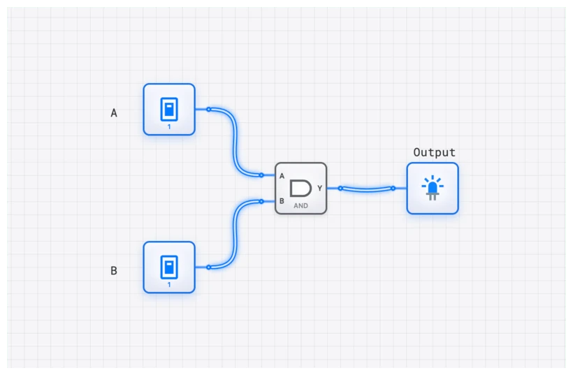
1. The AND Operation
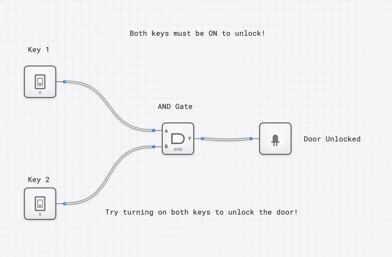
The output is TRUE (1) only when all inputs are TRUE. Think of it as a strict requirement: in a safety system for a heavy machine, you might want the motor to run only if the “Start Button” is pressed AND the “Safety Guard” is closed. In circuit terms, an AND gate acts as a series connection — every switch must be closed for current to flow.
- Boolean Expression:
- Component Name: AND
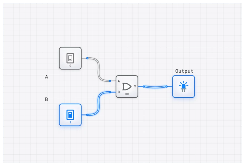
2. The OR Operation
The output is TRUE (1) if at least one input is TRUE. In a home security system, the alarm should trigger if the “Front Door Opens” OR the “Back Window Breaks.” In circuit terms, an OR gate acts as a parallel connection — current flows if any switch is closed.
- Boolean Expression:
- Component Name: OR
3. The NOT Operation (Inverter)
The output is the logical inverse of its single input. If the input is HIGH, the output is LOW, and vice versa. In circuit terms, a NOT gate (or inverter) flips the signal level, converting an active-high signal to active-low or back.
- Boolean Expression: (or )
- Component Name: NOT
When first learning these gates, a clean, isolated environment for toggling inputs and watching the truth table come to life is invaluable.
Technical Specifications: The Truth Tables
Truth tables are the fundamental scorecard of digital logic. They map every possible input combination to its resulting output.
AND Gate Truth Table
| Input A | Input B | Output Y |
|---|---|---|
| 0 | 0 | 0 |
| 0 | 1 | 0 |
| 1 | 0 | 0 |
| 1 | 1 | 1 |
OR Gate Truth Table
| Input A | Input B | Output Y |
|---|---|---|
| 0 | 0 | 0 |
| 0 | 1 | 1 |
| 1 | 0 | 1 |
| 1 | 1 | 1 |
NOT Gate Truth Table
| Input A | Output Y |
|---|---|
| 0 | 1 |
| 1 | 0 |
What Are the Laws of Boolean Algebra?
With our basic operations defined, we can now explore the laws that allow us to manipulate and simplify logical expressions. These are not abstract rules — they are circuit transformations. Each law corresponds to a concrete hardware optimization: removing a gate, eliminating a wire, or reducing propagation delay.
The Laws of Identity and Annihilation
These laws define how variables interact with the constants 0 and 1. You can verify them on digisim.io using the CONSTANT and CONSTANT_ZERO components.
- Identity Law: A variable combined with the identity element for its operation remains unchanged.
- OR with 0: — Tying one OR input to ground has no effect on the output.
- AND with 1: — Tying one AND input to VCC has no effect on the output.
- Null (Annihilation) Law: A variable combined with the dominant element yields that element.
- OR with 1: — If one OR input is permanently HIGH, the output is always HIGH regardless of A.
- AND with 0: — If one AND input is permanently LOW, the output is always LOW regardless of A.
The Laws of Complements and Idempotence
These laws govern how a variable interacts with itself or its inverse.
- Idempotent Law: Combining a variable with itself produces no change.
- — Wiring the same signal to both inputs of an OR gate is equivalent to a direct wire.
- — Wiring the same signal to both inputs of an AND gate is equivalent to a direct wire.
- Complement Law: A variable combined with its own inverse produces a constant.
- — A signal is always either HIGH or LOW, so one of the two OR inputs is always 1.
- — A signal cannot be both HIGH and LOW simultaneously, so the AND always outputs 0.
The Commutative, Associative, and Distributive Laws
For anyone coming from traditional algebra, most of these laws feel familiar.
- Commutative: and — The order of inputs to an AND or OR gate does not matter.
- Associative: and — You can cascade gates in any grouping; the result is the same.
- Distributive (Standard): — This works exactly as in ordinary algebra and lets you factor or expand expressions at will.
But Boolean algebra has a second distributive law with no counterpart in the algebra of real numbers.
This is counterintuitive at first. In regular math, , while . They are not equal. But in the binary world of Boolean logic, this identity holds.
The key to intuition: if , both sides evaluate to 1 immediately. If , both sides reduce to . Do not try to “FOIL” the right side as you would a quadratic — Boolean algebra has no notion of squared terms, since . This second distributive law is the cornerstone of converting between Sum-of-Products (SOP) and Product-of-Sums (POS) forms, which are the two canonical representations of any Boolean function.
The Power Tools: Absorption and De Morgan’s Laws
The following laws eliminate entire terms and radically restructure expressions. They are the workhorses of real-world circuit simplification.
The Absorption Law: Eliminating Redundancy
The Absorption Law lets you delete entire gates from your design without changing behavior.
The intuition for the first form: is true if is true, OR if both and are true. But if is already true, the entire expression is true regardless of . The term is completely redundant. In hardware, this eliminates an AND gate and an OR gate, replacing them with a direct wire.
There is also a lesser-known variant sometimes called the Consensus Theorem:
The third term () is redundant because it is already covered by the other two terms in every case. This is harder to spot by inspection, but a Karnaugh map makes it visually obvious.
De Morgan’s Laws: Distributing Negation
Augustus De Morgan’s theorems show how to distribute a NOT operation across ANDs and ORs, enabling you to restructure inverted expressions.
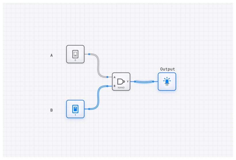
- First Law: — A NAND gate is equivalent to an OR gate with inverted inputs.
- Second Law: — A NOR gate is equivalent to an AND gate with inverted inputs.
In circuit terms, this duality is fundamental to modern chip design. In CMOS technology, NAND and NOR gates are physically smaller and faster than standard AND and OR gates, so designers routinely use De Morgan’s Laws to convert logic into NAND-only or NOR-only implementations. For a deeper treatment, see our dedicated article on applying De Morgan’s Laws in practice.
Simulating on digisim.io: From Theory to Tangible Proof
Reading about these laws is one thing; seeing them work is another. Let’s prove the Absorption Law, , on the digisim.io canvas.
Step-by-Step Verification
- Open the Simulator: Start a new project at digisim.io/circuits/new.
- Place Inputs: Drag two INPUT_SWITCH components onto the canvas. Label them ‘A’ and ‘B’ using the TEXT tool.
- Build the Complex Side:
- Place an AND gate. Connect ‘A’ and ‘B’ to its inputs.
- Place an OR gate. Connect the output of the AND gate to one input, and connect ‘A’ directly to the other input.
- Connect the OR gate’s output to an OUTPUT_LIGHT.
- Build the Simplified Side:
- Simply connect ‘A’ directly to a second OUTPUT_LIGHT.
- The SimCast Moment: Use the SimCast feature to record your interaction. Toggle ‘A’ and ‘B’ through all four combinations. You will notice that the two lights always match. No matter what ‘B’ does, the first light only cares about ‘A’.
Oscilloscope Verification: Watching the Propagation
To truly understand the “cost” of the unsimplified circuit, place an OSCILLOSCOPE_8CH on the canvas. Connect Channel 1 to Input ‘A’ and Channel 2 to the output of your complex OR gate.
When you toggle ‘A’, you will see a tiny delay in the waveform on the oscilloscope. This is the propagation delay (). Every gate adds a small amount of time for the signal to propagate. By simplifying down to just , you remove the delay of two gates (the AND and the OR), reducing the total from to zero. In high-speed designs, these savings directly translate to higher achievable clock frequencies.
The Security Alarm template demonstrates how multiple gates (AND, OR, NOT) work together in a real-world context — a useful playground for applying simplification laws.
Real-World Application: Where Simplification Saves the Day
This isn’t just about saving a few gates in a classroom exercise. In real-world systems, simplification directly translates to cheaper, faster, and more power-efficient hardware.
Example 1: High-Speed Memory Address Decoding
In the classic Intel 8086 architecture, the CPU uses address lines to select which memory chip to talk to. The logic that enables a specific chip is called an address decoder. If the decoder logic is unoptimized, it takes longer for the “Enable” signal to reach the RAM chip. This forces the CPU to insert “wait states”—essentially idling because the logic is too slow. By applying Boolean laws to the decoder circuitry, engineers can shave off enough delay to run the entire system at a higher clock speed.
Example 2: The ALU Status Flags
The Arithmetic Logic Unit (ALU) is the computational heart of a CPU. After an operation, it sets status flags in the FLAGS_REGISTER (like Zero, Negative, or Overflow). The logic for the Overflow flag is notoriously complex, involving the carry-in and carry-out of the most significant bits.
If you were to build this using raw logic without simplification, you’d end up with a massive web of gates. By using De Morgan’s laws and the Distributive property, designers can compress this logic into a few high-speed NAND gates, ensuring the flags are ready the instant the calculation finishes.
Related Topics in the Curriculum
As you continue exploring digital logic on digisim.io, these related topics will deepen your understanding:
- Digital Logic 101: AND, OR, NOT gates
- Logic Gate Truth Tables: Reference
- De Morgan’s Laws in Practice
- Karnaugh Maps for Visual Simplification
- Sum of Products (SOP) and Product of Sums (POS)
Quick Reference: All Laws at a Glance
| Law | OR Form | AND Form |
|---|---|---|
| Identity | ||
| Null | ||
| Idempotent | ||
| Complement | ||
| Commutative | ||
| Associative | ||
| Distributive | ||
| Absorption | ||
| De Morgan’s | ||
| Double Negation |
Your Turn: Put Knowledge into Practice
Boolean algebra is the language that bridges the gap between an abstract idea and a functioning piece of silicon. These laws are the mathematical tools you use to sculpt logic, eliminate waste, and create designs that are as efficient as they are correct.
Here is a challenge: take the expression .
- Factor out common terms using the Distributive Law: .
- Apply the Complement Law () and the Identity Law () to get .
- Factor again: . (The last step uses the absorption variant .)
- Open digisim.io and build both the original 3-minterm circuit and the simplified 2-gate version.
- Use an OSCILLOSCOPE to compare the propagation delay.
Continue with the next entry in this series: Sum of Products (SOP), or open the AND gate component reference to wire one of these laws yourself.