Mastering Binary Addition: Building a 4-Bit Ripple Carry Adder
A 4-bit ripple carry adder chains four full adders to add multi-bit numbers. Covers architecture, propagation delay, overflow detection, and a build.

TL;DR: A 4-bit ripple carry adder chains four full adders so each stage’s carry-out feeds the next stage’s carry-in. The architecture is simple but slow: total propagation delay scales linearly as , which is why high-speed CPUs use carry-lookahead adders instead.
The natural next step after a single full adder is multi-bit addition. Adding two 4-bit numbers like and requires four full adders chained together so a carry generated in one column can propagate to the next.
This is the 4-bit ripple carry adder — the first “complex” system most students build, where the theoretical beauty of Boolean algebra meets the physical reality of propagation delay. This guide builds one from chained components, derives the delay formula, and shows how to detect overflow.
What is a Ripple Carry Adder?
At its core, a ripple carry adder is a combinational logic circuit that produces the arithmetic sum of two binary numbers. While a single FULL_ADDER handles three inputs (two bits plus a carry-in) and produces two outputs (sum and carry-out), a 4-bit adder must handle two 4-bit words.
The “ripple” part of the name describes the behavior of the carry bit. In a multi-bit addition, the carry generated at the least significant bit (LSB) must be passed to the next bit, which might then generate a carry for the next, and so on. The carry literally “ripples” through the chain of adders from right to left.
In the digisim.io ecosystem, we treat the FULL_ADDER as our fundamental building block for this hierarchy. By the time you reach the advanced topics in our curriculum, you’ll realize that almost all digital arithmetic is just a clever arrangement of these blocks.
The Architecture of the Chain
To build a 4-bit adder, we need four FULL_ADDER components. Let’s label our inputs as (bits ) and (bits ).
- Stage 0 (LSB): Takes , , and a (usually tied to CONSTANT_ZERO).
- Stage 1: Takes , , and the from Stage 0.
- Stage 2: Takes , , and the from Stage 1.
- Stage 3 (MSB): Takes , , and the from Stage 2.
The final output consists of four sum bits () and one final carry-out (), which represents an overflow in unsigned 4-bit arithmetic.
Technical Specification: The Truth Table
While a full truth table for a 4-bit adder would require rows (512 entries!), we can look at critical test cases to verify our logic.
| A (Dec) | B (Dec) | A (Bin) | B (Bin) | Sum (Bin) | Result (Dec) | |
|---|---|---|---|---|---|---|
| 0 | 0 | 0000 | 0000 | 0000 | 0 | 0 |
| 7 | 1 | 0111 | 0001 | 1000 | 0 | 8 |
| 9 | 6 | 1001 | 0110 | 1111 | 0 | 15 |
| 15 | 1 | 1111 | 0001 | 0000 | 1 | 16 (Overflow) |
| 15 | 15 | 1111 | 1111 | 1110 | 1 | 30 (Overflow) |
The Boolean Foundation
Each stage of our ripple carry adder is governed by two primary equations. For any bit :
Sum Equation:
Carry-Out Equation:
In digisim.io, you can see these equations in action by looking at the internal gates of a FULL_ADDER. It typically uses two XOR gates for the sum and a combination of AND/OR gates for the carry logic.
Common Pitfall: The Propagation Delay Bottleneck
In a simulator, signals can feel instantaneous. In real silicon and high-fidelity simulations, they are not. See propagation delay for the physics behind this.
The ripple carry adder is notoriously slow. Why? Because Stage 3 cannot calculate its final sum until Stage 2 provides a carry. Stage 2 is waiting on Stage 1, and Stage 1 is waiting on Stage 0.
If each FULL_ADDER’s carry path has a propagation delay () of 2 nanoseconds, a 4-bit adder takes 8ns for the carry to stabilize. That doesn’t sound like much, but imagine a 64-bit ripple carry adder in a modern CPU. You’d be looking at 128ns just for one addition. At a 3GHz clock speed, your CPU cycle is only 0.33ns. The math simply doesn’t work.
The Ripple Delay Formula:
For an -bit ripple carry adder, the worst-case total propagation delay is:
This linear relationship between bit width and delay is the fundamental weakness of the ripple carry architecture. It is precisely why the Carry Lookahead Adder (CLA) was invented. A CLA uses additional “generate” () and “propagate” () signals to compute all carry bits simultaneously from the original inputs, reducing the delay from to at the cost of more complex gate logic.
When you are debugging your circuit in digisim.io, if you see the outputs flickering briefly when you change the inputs, you are witnessing the settling time of the ripple carry.
Building the Circuit in digisim.io
Let’s get hands-on. Follow these steps to build your own 4-bit arithmetic unit:
- Place the Inputs: Use two sets of four INPUT_SWITCH components. Label them and .
- Add the Logic: Drop four FULL_ADDER components onto the canvas.
- The Carry Chain: Connect the of the first adder to the of the second. Repeat this for all four stages.
- Ground the First Carry: Connect the of the LSB adder to a CONSTANT_ZERO.
- Visualize the Output: Connect the four Sum outputs to a DIGIT_DISPLAY or four OUTPUT_LIGHT components. Connect the final to a separate “Overflow” light.
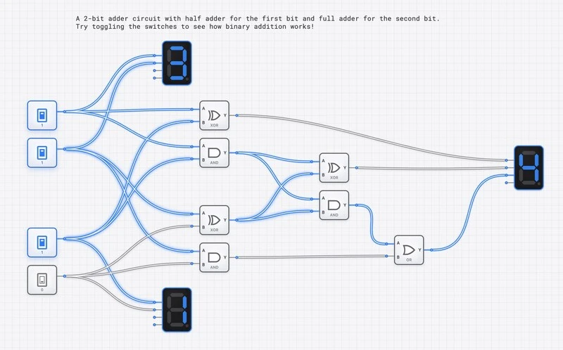
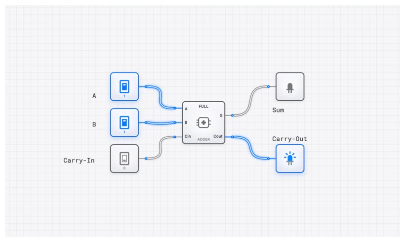
Note: While the image above shows a 2-bit version, the principle for the 4-bit version is identical—just keep chaining!
Verifying with the OSCILLOSCOPE_8CH
To see the “ripple” effect, connect an OSCILLOSCOPE_8CH to your circuit and capture each stage’s carry-out as inputs change.
- Channel 1: (The trigger)
- Channel 2: of Stage 0
- Channel 3: of Stage 1
- Channel 4: of Stage 2
- Channel 5: of Stage 3
When you toggle from LOW to HIGH while are all HIGH, you will see a staggered “staircase” effect on the oscilloscope. Each channel will go HIGH slightly after the one before it. This is the physical manifestation of the ripple delay. If your clock speed is too high, the next operation might start before the carry has finished rippling to the end!
Real-World Applications and ICs
In the 1970s and 80s, engineers didn’t build these from individual gates; they used dedicated Integrated Circuits (ICs). The most famous is the 74LS283.
The 74LS283 is a high-speed 4-bit binary full adder. Interestingly, internally it doesn’t use a pure ripple carry. It uses a technique called Carry Lookahead logic. Instead of waiting for the carry to ripple, it uses extra gates to “predict” if a carry will be generated based on all the inputs simultaneously. This makes it significantly faster than the circuit we just built, though the logical result is exactly the same.
You’ll find these adders at the heart of:
- The Intel 8086: The grandfather of modern PC processors used similar adder structures in its ALU.
- Game Boys: The Sharp LR35902 processor inside the original Game Boy relied on 8-bit addition circuits to handle sprite coordinates and game logic.
Advanced Concept: Overflow Detection
How do we know if our 4-bit adder has “failed” because the number is too big?
For unsigned numbers, it’s easy: if the final is 1, you have an overflow. For signed numbers (Two’s Complement), it’s trickier. A signed overflow occurs if the carry into the MSB is different from the carry out of the MSB.
Signed Overflow Formula:
If you’re following our structured learning path on digisim.io, we dive deep into this in Signed Arithmetic and Overflow. It’s a crucial concept for preventing bugs like the famous “Year 2038” problem or integer wraps in video games.
Summary and Next Steps
The 4-bit ripple carry adder is a rite of passage for any digital designer. It teaches you that logic isn’t just about truth tables; it’s about the flow of data through time.
By chaining FULL_ADDER components, you’ve moved from simple gates to a functional arithmetic unit. You’ve also encountered the primary enemy of high-speed computing: propagation delay.
Ready to put this into practice?
- Open digisim.io and build the 4-bit adder from scratch.
- Try adding and watch the carry ripple through all four stages.
- Connect a SEVEN_SEGMENT_DISPLAY through a BCD decoder to see the decimal results.
Continue with the fetch-decode-execute cycle to see how this ALU primitive plugs into a CPU, or open the FULL_ADDER component reference directly.