Every app on your phone, every search result Google returns, every frame of video streaming to your screen begins as a sequence of electrical pulses moving through circuits at near-light speed. Those pulses represent the simplest possible distinction: on or off, 1 or 0, true or false. The field that studies how to harness these pulses to perform computation is called digital logic, and it is the foundation on which all modern computing is built.
This post is your orientation. We will cover what digital logic actually is, why binary is the medium of choice, how the core logic gates work, and where this discipline fits in the broader landscape of computer science and electrical engineering. By the end, you will have a conceptual map of the territory ahead.
What Is Digital Logic?
Digital logic is the branch of electronics that deals with signals restricted to discrete values, most commonly two: HIGH and LOW (1 and 0). Unlike analog circuits, where a voltage can take any value along a continuous spectrum, digital circuits snap every signal into one of two well-defined states. This constraint is not a limitation; it is the source of digital systems’ extraordinary reliability.
The distinction matters because of noise. Every physical wire picks up electromagnetic interference, thermal fluctuations, and crosstalk from neighboring wires. In an analog system, each disturbance directly corrupts the signal. In a digital system, a signal only needs to be recognized as “closer to HIGH” or “closer to LOW.” As long as the noise does not push a 0 past the threshold into 1 territory (or vice versa), the information is preserved perfectly. This is why you can copy a digital file a million times with zero degradation, while a photocopy of a photocopy quickly turns to mush.
Why Binary? The Case for Two States
At first glance, restricting yourself to two values seems wasteful. Why not use ten voltage levels and encode a full decimal digit per wire? The answer involves physics, mathematics, and engineering pragmatism.
The Physics Argument
Transistors, the microscopic switches at the heart of every chip, are most reliable when operated in saturation (fully on) or cutoff (fully off). Operating them in intermediate states introduces heat, increases error rates, and complicates circuit design. Binary exploits the transistor’s natural strengths.
The Noise Margin Argument
With only two states, you can separate them by a wide voltage gap. In a 5V system, anything above roughly 3.5V counts as HIGH and anything below about 1.5V counts as LOW. That leaves a 2V margin for noise. If you tried to distinguish ten levels within the same 5V range, each level would get only 0.5V of margin, and a small fluctuation could corrupt data.
The Mathematical Argument
In 1854, mathematician George Boole published The Laws of Thought, formalizing a system of algebra where variables take only the values TRUE and FALSE and are combined through operations like AND, OR, and NOT. Nearly a century later, Claude Shannon’s 1937 master’s thesis demonstrated that Boole’s algebra maps directly onto electrical switching circuits. Binary is not just convenient; it has a rigorous mathematical framework ready-made for circuit design.
The Binary Number System
If each wire can only carry a 0 or a 1, how do we represent larger numbers? The same way the decimal system works, but with a base of 2 instead of 10.
In decimal (base 10), the number 157 means:
In binary (base 2), the number 10011101 means:
Each binary digit is called a bit. Eight bits form a byte, which can represent values from 0 to 255 (that is, ). A 32-bit integer can represent over 4 billion distinct values. The entire richness of modern computing, from text to images to neural network weights, is encoded as structured collections of bits.
A Quick Conversion Reference
| Decimal | Binary | Bits Required |
|---|---|---|
| 0 | 0 | 1 |
| 1 | 1 | 1 |
| 5 | 101 | 3 |
| 10 | 1010 | 4 |
| 15 | 1111 | 4 |
| 255 | 11111111 | 8 |
Logic Gates: The Vocabulary of Digital Circuits
Once you have binary signals, you need a way to combine and transform them. That is the job of logic gates. A logic gate takes one or more binary inputs and produces a single binary output according to a fixed rule. There are three fundamental gates from which all others can be derived.
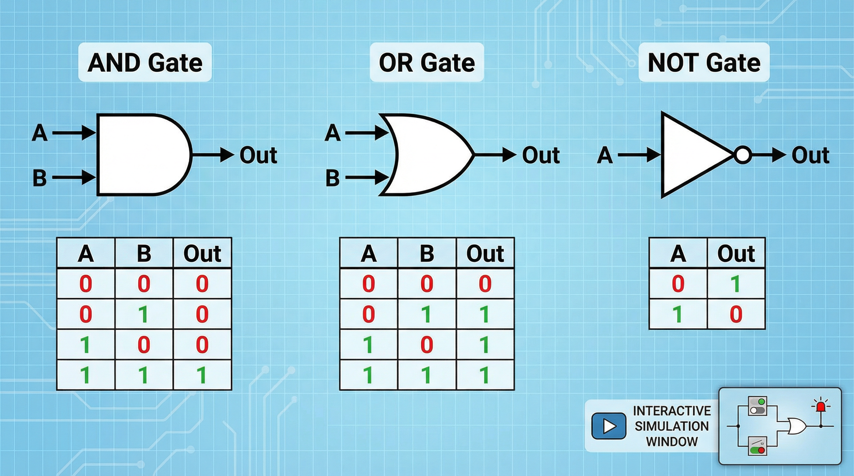
The AND Gate
The AND gate outputs 1 only when all of its inputs are 1. If any input is 0, the output is 0. Think of it as a security checkpoint that requires every credential to be valid before granting access.
| Input A | Input B | Output Y |
|---|---|---|
| 0 | 0 | 0 |
| 0 | 1 | 0 |
| 1 | 0 | 0 |
| 1 | 1 | 1 |
Boolean expression:
The AND operation behaves like multiplication: any factor of zero forces the product to zero.
The OR Gate
The OR gate outputs 1 when at least one input is 1. It outputs 0 only when all inputs are 0. This is the logic behind any system where multiple triggers can produce the same response, like an emergency stop system with buttons at several locations.
| Input A | Input B | Output Y |
|---|---|---|
| 0 | 0 | 0 |
| 0 | 1 | 1 |
| 1 | 0 | 1 |
| 1 | 1 | 1 |
Boolean expression:
Note that this is logical OR, not arithmetic addition. In Boolean algebra, .
The NOT Gate (Inverter)
The NOT gate has a single input and simply flips it. A 1 becomes a 0, and a 0 becomes a 1. Despite its simplicity, the NOT gate is indispensable. Without inversion, you cannot construct circuits that negate conditions, and negation turns out to be essential for general-purpose computation.
| Input A | Output Y |
|---|---|
| 0 | 1 |
| 1 | 0 |
Boolean expression:
From Three Gates to Everything
A remarkable result in digital logic is that AND, OR, and NOT together are functionally complete: any Boolean function, no matter how complex, can be expressed using only these three operations. In practice, engineers also use derived gates like NAND (AND followed by NOT), NOR (OR followed by NOT), and XOR (exclusive OR), but these are all compositions of the three primitives.
Even more remarkably, the NAND gate alone is functionally complete. Every gate, including AND, OR, and NOT, can be built using only NAND gates. This is why NAND is sometimes called the “universal gate” and why most integrated circuits are implemented primarily in NAND-based logic.
Boolean Algebra: The Mathematics of Logic
George Boole’s algebra gives us a formal system for reasoning about digital circuits on paper before we ever build them. A few essential laws:
Identity Laws:
Null Laws:
Complement Laws:
De Morgan’s Theorems:
De Morgan’s theorems are particularly powerful. They tell you that a NAND gate (inverting an AND) is equivalent to an OR gate with inverted inputs, and vice versa. This equivalence is the basis for converting between different gate implementations and is one of the most-used tools in circuit optimization.
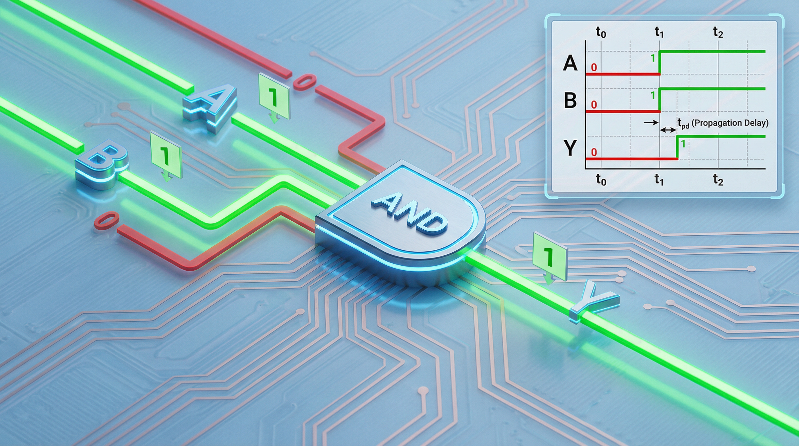
Propagation Delay: Where Physics Meets Logic
In textbook diagrams, gates respond to their inputs instantaneously. In physical circuits, every gate has a propagation delay (), typically measured in nanoseconds, caused by the finite time transistors need to switch states.
For a single gate, this delay is negligible. But modern processors chain millions of gates together in series. If the longest path through a circuit (the critical path) has a total propagation delay of 2 nanoseconds, the circuit cannot be clocked faster than 500 MHz without risking incorrect results. Understanding and minimizing critical-path delay is one of the central challenges of high-performance circuit design.
When signals travel through paths of different lengths and arrive at a gate at slightly different times, the gate may briefly produce an incorrect output known as a glitch. Managing these timing hazards is a skill that distinguishes working prototypes from production-ready designs.
Seeing It in Action: Simulation on digisim.io
Theory builds understanding, but experimentation builds intuition. On digisim.io, you can build and test any of the circuits described above in seconds.
- Start a new circuit at digisim.io.
- Place two Input Switches and one AND Gate from the component palette.
- Wire each switch to an input of the AND gate.
- Add an Output Light and wire the AND gate’s output to it.
- Toggle the switches and verify the truth table row by row.
Then try replacing the AND gate with an OR gate and observe how the behavior changes. Finally, place a NOT gate between a switch and a light to see inversion firsthand. In a few minutes, you will have verified every truth table in this article through direct experimentation.
Where Digital Logic Fits: The Abstraction Stack
Understanding digital logic means understanding where you stand in computing’s hierarchy of abstraction:
- Physics — Semiconductor behavior, electron flow, voltage thresholds.
- Transistors — Individual switches built from semiconductors.
- Logic Gates — Small groups of transistors implementing Boolean functions. You are here.
- Combinational Circuits — Gates combined to perform operations like addition, comparison, and multiplexing.
- Sequential Circuits — Circuits with memory (flip-flops, registers) that maintain state.
- Functional Units — ALUs, register files, control units.
- Processor Architecture — Complete CPUs built from functional units.
- Software — Operating systems, applications, and everything above.
Every layer is built entirely from the layer below it. The CPU executing your web browser is, at bottom, billions of AND, OR, and NOT gates switching in coordinated patterns at gigahertz frequencies. Learning digital logic means learning the layer where abstract mathematics first becomes physical reality.
Real-World Applications
Digital logic is not confined to textbooks. It appears anywhere decisions must be made in hardware:
- Memory address decoding uses AND gates to select one memory chip out of many based on the pattern of address bits.
- Error detection in network protocols uses XOR gates to compute parity bits, catching single-bit transmission errors.
- Arithmetic circuits in every processor use cascaded full adders, each built from AND, OR, and XOR gates, to perform binary addition.
- Safety interlocks in industrial equipment use AND logic to require multiple conditions (two-hand operation, guard closed, emergency stop released) before enabling dangerous machinery.
- Autonomous vehicles process sensor data through hardware logic pipelines for time-critical decisions where software latency is unacceptable.
What Comes Next
This article has given you the conceptual foundation. From here, the standard curriculum progresses through:
- Mastering each gate — AND, OR, NOT, NAND, NOR, XOR, XNOR in depth.
- Combinational design — Building adders, multiplexers, decoders, and encoders.
- Sequential design — Flip-flops, counters, registers, and finite state machines.
- Processor architecture — Combining everything into a working CPU.
Each step builds directly on the last, and every step can be practiced hands-on with simulation. The gap between reading about a half adder and building one yourself is where real learning happens.
Ready to take the first step? Open digisim.io, build an AND gate circuit, verify its truth table, then challenge yourself: can you make a circuit whose output is 1 only when exactly one of two inputs is 1? (Hint: that is the XOR function, and building it from AND, OR, and NOT gates is a rite of passage in digital logic education.)