Visualizing the Fetch-Decode-Execute Cycle in a Simulator
Step through every microoperation of a CPU's fetch-decode-execute cycle: program counter, instruction register, ALU, and control unit at the bit level.

TL;DR: Every CPU executes instructions through a three-phase loop: fetch (read instruction from memory using the Program Counter), decode (the Control Unit interprets the opcode), and execute (the ALU and register file carry out the operation). Watching this loop step-by-step in a simulator turns the abstract cycle into observable bits and signals.
The CPU executes every program by repeating the same fundamental three-step process billions of times per second: fetch an instruction from memory, decode it to determine what operation to perform, and execute that operation. This fetch-decode-execute cycle is the heartbeat of computation.
Yet the cycle is notoriously difficult to teach. On real hardware, it completes in nanoseconds, making it invisible to human observation. Static diagrams in textbooks show the data paths but fail to convey the dynamic, step-by-step flow of bits through the processor. Interactive simulation closes that gap by exposing every transfer between the program counter, instruction register, and ALU.
What Are the Key Components of a CPU?
Before tracing an instruction, we need to understand the hardware components involved. A minimal CPU contains:
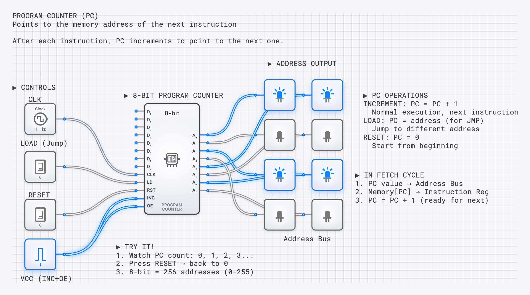
- Program Counter (PC): A register that holds the memory address of the next instruction to fetch. It increments automatically after each fetch, pointing the CPU to the next instruction in sequence.
- Memory Address Register (MAR): Holds the address being sent to memory. The PC’s value is copied here during a fetch.
- Memory (RAM): Stores both instructions and data as binary values at numbered addresses.
- Memory Data Register (MDR): Holds the data read from (or to be written to) memory.
- Instruction Register (IR): Stores the instruction currently being executed. The fetched instruction is loaded here from the MDR.
- Control Unit (CU): Decodes the instruction in the IR and generates the control signals that orchestrate all other components.
- Arithmetic Logic Unit (ALU): Performs arithmetic (built from circuits like the 4-bit ripple-carry adder) and logical (AND, OR, XOR) operations on data.
- Register File: A small set of fast storage locations (R0, R1, R2, etc.) — built from arrays of 4-bit registers — that hold the data the CPU is currently working with.
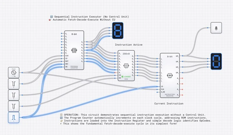
DigiSim.io’s Sequential Instruction Executor: a working CPU simulation where students can watch every stage of instruction processing.
Instruction Format: How Instructions Are Encoded
Every instruction the CPU executes is a binary number stored in memory. The bits of this number are divided into fields, each with a specific purpose. Our example CPU uses two 16-bit instruction formats:
Format A — Register-mode (used by ADD, SUB, AND):
| 15  14  13  12 | 11  10  9  8 | 7  6  5  4 | 3  2  1  0 |
| OPCODE | REG_A | REG_B | REG_D |- Opcode (bits 15-12): A 4-bit code identifying the operation. With 4 bits, we can define up to 16 different instructions.
- REG_A (bits 11-8): The address of the first source register.
- REG_B (bits 7-4): The address of the second source register.
- REG_D (bits 3-0): The address of the destination register where the result is stored.
Format B — Immediate-mode (used by LOAD-immediate):
| 15  14  13  12 | 11  10  9  8 |  7  6  5  4  3  2  1  0  |
|    OPCODE      |    REG_D     |        IMMEDIATE          |
LOAD-immediate uses bits 11-8 for the destination register and the lower 8 bits as a signed/unsigned immediate value.
Example opcodes for our simple CPU:
| Opcode | Binary | Format | Operation |
|---|---|---|---|
| LOAD | 0001 | B | Load an immediate value into REG_D |
| ADD | 0010 | A | REG_D ← REG_A + REG_B |
| SUB | 0011 | A | REG_D ← REG_A − REG_B |
| AND | 0100 | A | REG_D ← REG_A & REG_B |
| STORE | 0101 | A | Store REG_A to memory at REG_B |
| HALT | 1111 | — | Stop execution |
The Three Phases in Detail
Phase 1: FETCH — Getting the Instruction
The fetch phase retrieves the next instruction from memory. Here is what happens at the bit level, step by step:
- PC to MAR: The current value of the Program Counter is copied into the Memory Address Register. If , then . The address bus now carries this value to the memory module.
- Memory read: The memory module receives the address on the address bus and places the contents of that address onto the data bus. If address contains the value , then the data bus carries .
- MDR load: The Memory Data Register captures the value from the data bus: .
- IR load: The value in the MDR is transferred to the Instruction Register: . The instruction is now inside the CPU, ready for decoding.
- PC increment: The Program Counter increments by 1 (or by the instruction width in byte-addressable systems): . This prepares the CPU to fetch the next instruction in the following cycle.
The fetch phase is the same for every instruction. The CPU does not yet know what the instruction means; it has only retrieved the raw binary data.
Phase 2: DECODE — Understanding the Instruction
The decode phase interprets the binary instruction. The Control Unit examines the fields of the IR and generates the appropriate control signals:
- Extract the opcode: . The CU recognizes this as the ADD operation (Format A).
- Extract the register addresses:
- : Read from register R0 (source A).
- : Read from register R1 (source B).
- : Write the result to register R2 (destination).
- Activate the register file: The CU sends the source register addresses to the register file’s read ports. If and , the read ports output and .
- Configure the ALU: The CU sends an ALU control signal corresponding to ADD. The ALU is now ready to perform addition on whatever appears at its inputs.
No computation has occurred yet. The decode phase only sets up the data paths and control signals so that the execute phase can proceed.
Phase 3: EXECUTE — Performing the Operation
The execute phase carries out the operation specified by the instruction:
- ALU operation: The two operand values from the register file (R0 = 5 and R1 = 3 in our example) arrive at the ALU inputs. The ALU performs the ADD operation: .
- Status flags update: The ALU updates its condition flags:
- Zero (Z) = 0: The result is not zero.
- Carry (C) = 0: No carry out of the most significant bit.
- Negative (N) = 0: The result is positive (MSB is 0).
- Overflow (V) = 0: No signed overflow occurred.
- Write-back: The ALU result (8, or binary ) is written to the destination register R2. The register file’s write port receives the destination address (0010 = R2) and the data value.
The instruction is now complete. The CPU loops back to the fetch phase, where the incremented PC points to the next instruction at address .
SimCast lesson showing each phase of the cycle with highlighted data paths and explanatory annotations.
Complete Walkthrough: A Three-Instruction Program
Let us trace a complete program that loads two values and adds them. The program resides in memory starting at address :
| Address | Instruction (Hex) | Format | Assembly | Meaning |
|---|---|---|---|---|
| 0x00 | 0x1005 | B | LOAD R0, #5 | — opcode 0001, REG_D=0, IMM=5 |
| 0x01 | 0x1103 | B | LOAD R1, #3 | — opcode 0001, REG_D=1, IMM=3 |
| 0x02 | 0x2012 | A | ADD R2, R0, R1 | — opcode 0010, REG_A=0, REG_B=1, REG_D=2 |
Cycle 1: Execute LOAD R0, #5
- Fetch: PC=0x00. Memory returns 0x1005. IR=0x1005. PC increments to 0x01.
- Decode: Opcode = 0001 (LOAD, Format B). REG_D = (R0). IMM = (5).
- Execute: The immediate value 5 is written to R0. .
Cycle 2: Execute LOAD R1, #3
- Fetch: PC=0x01. Memory returns 0x1103. IR=0x1103. PC increments to 0x02.
- Decode: Opcode = 0001 (LOAD, Format B). REG_D = (R1). IMM = (3).
- Execute: The immediate value 3 is written to R1. .
Cycle 3: Execute ADD R2, R0, R1
- Fetch: PC=0x02. Memory returns 0x2012. IR=0x2012. PC increments to 0x03.
- Decode: Opcode = 0010 (ADD, Format A). Source A = R0, Source B = R1, Destination = R2. The register file outputs R0=5 and R1=3.
- Execute: ALU computes . The result is written to R2. .
After three cycles, the CPU has loaded two constants and computed their sum. The result 8 sits in register R2, ready for further computation or output.
The Program Counter: More Than Just an Incrementer
In the examples above, the PC simply incremented by 1 after each fetch. But the PC is also the mechanism for branching and jumping. A branch instruction (like “jump to address 0x00 if the Zero flag is set”) works by writing a new value directly into the PC during the execute phase. Instead of incrementing, the PC is loaded with the branch target address, causing the CPU to fetch its next instruction from a completely different location in memory.
This is how loops, conditionals, and function calls work at the hardware level. A for loop in a high-level language compiles down to a conditional branch instruction that resets the PC to the top of the loop body until the loop counter reaches its limit.
Memory Addressing and the Address Space
The Program Counter and memory work together through a system of addresses. Each location in memory has a unique numerical address, starting from 0. When the CPU needs to fetch an instruction, it places the address on the address bus, a set of parallel wires that carry the binary address to the memory module.
The width of the address bus determines the maximum number of memory locations the CPU can access. An 8-bit address bus can address locations. A 16-bit address bus addresses locations — 64 KB if memory is byte-addressable, 128 KB if memory is word-addressable (each location holding a 16-bit word). This is the CPU’s address space.
Similarly, the data bus carries the actual instruction or data value between the CPU and memory. Its width determines how many bits can be transferred in a single memory access. In our example, the data bus is 16 bits wide, matching our instruction word size.
In the digisim.io Sequential Instruction Executor, you can observe both buses simultaneously. During a fetch, the address bus carries the PC value while the data bus carries the instruction being read. During a memory store instruction, the address bus carries the target memory address while the data bus carries the value being written.
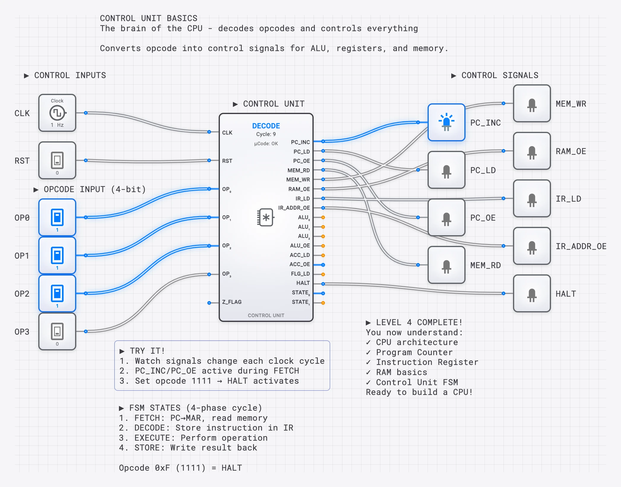
How the Control Unit Orchestrates the Cycle
The Control Unit is the conductor of the CPU orchestra. It does not perform any computation itself; instead, it generates control signals that tell every other component what to do at each step.
During the fetch phase, the CU asserts signals like:
- PC_to_MAR: Copy the PC value to the Memory Address Register.
- MEM_READ: Tell memory to output the contents of the addressed location.
- MDR_to_IR: Load the value from the data bus into the Instruction Register.
- PC_INC: Increment the Program Counter.
During decode and execute, the CU generates different signals based on the opcode:
- ALU_OP: A multi-bit signal specifying which ALU operation to perform (ADD, SUB, AND, etc.).
- REG_READ_A, REG_READ_B: Specify which registers to read.
- REG_WRITE: Specify the destination register and enable writing.
- MEM_WRITE: For store instructions, enable writing to memory.
Each instruction type activates a unique combination of these signals. The CU is essentially a decoder that translates opcodes into the specific control signal patterns that make each instruction work.
The Power of Slow Motion
Real CPUs execute billions of cycles per second. The entire three-instruction program above would complete in roughly one nanosecond on a modern processor. This speed makes the internal mechanics invisible.
Interactive simulation inverts this relationship. On digisim.io, you can:
- Step one clock cycle at a time, watching each phase unfold.
- Observe the binary values on every bus, register, and control line as they change.
- Trace the data path visually, seeing which wires are active (carrying a signal) and which are idle.
- Predict what happens next before advancing the clock, turning passive observation into active learning.
A complete Simple CPU lesson where students can modify the program and observe execution.
Exercise: Trace an Instruction Yourself
Open the Sequential Instruction Executor template on digisim.io and try the following exercise:
- Load a program into memory. Start with the three-instruction program above (LOAD 5, LOAD 3, ADD).
- Reset the CPU so that PC = 0x00.
- Step through each clock cycle. For each cycle, write down:
- What value is on the address bus?
- What value is on the data bus?
- What does the IR contain?
- What control signals are active?
- What is the ALU doing?
- Modify the program. Change the ADD to a SUB and predict what R2 will contain. Then step through to verify.
- Add a branch instruction. Insert a “jump to 0x00” at address 0x03 to create an infinite loop. Watch the PC reset to 0x00 after the jump executes.
This exercise transforms the fetch-decode-execute cycle from an abstract concept into a concrete, observable process.
Classroom Implementation
Live Demonstration (15 minutes)
- Open the Sequential Instruction Executor template.
- Load a simple program (load constant, add, store).
- Step through each cycle, narrating the data flow.
- Ask students to predict what happens next before each step.
Hands-On Lab Exercise
- Students open the simulation individually.
- Provide a mystery program as raw binary values (no assembly mnemonics).
- Students decode each instruction manually by extracting opcodes and operand fields.
- They verify their decoding by stepping through the simulation and comparing predictions to actual behavior.
- Students write their own simple program and test it.
Understanding Timing: Clock Cycles and Microoperations
Each phase of the fetch-decode-execute cycle does not happen instantaneously. In a simple (non-pipelined) CPU, each phase occupies one or more clock cycles. During each clock cycle, one or more microoperations execute in parallel.
For example, the fetch phase might break down into three clock cycles:
- T0: (copy PC to MAR, assert memory-read)
- T1: (memory drives the data bus; MDR captures the result)
- T2: , (load instruction register and increment PC simultaneously)
The decode and execute phases similarly decompose into microoperations. A simple ADD instruction might complete in one execute cycle, while a memory store instruction might require two (one to compute the address, one to write the data).
The total number of clock cycles per instruction is called the CPI (Cycles Per Instruction). A simple CPU might have a CPI of 3-5. Modern pipelined processors achieve an effective CPI approaching 1 (or even less than 1 with superscalar execution) by overlapping the phases of multiple instructions.
In the digisim.io simulation, each clock step advances by one microoperation, making it possible to observe exactly which registers change at each sub-step of the cycle.
Advanced Topics Enabled
Once students master the basic cycle, the same simulation platform opens the door to more advanced concepts:
- Pipelining: What happens when fetch, decode, and execute overlap? The CPU can start fetching instruction while still executing instruction .
- Branching and pipeline hazards: A branch instruction invalidates the already-fetched next instruction, requiring a “pipeline flush.”
- Interrupts: An external signal forces the CPU to save its current PC, jump to an interrupt handler, and later resume execution.
- Memory hierarchy: What happens when the fetch phase must wait for data to arrive from slow main memory instead of fast cache?
Each of these topics builds directly on the fundamental cycle. If the student understands how bits flow through the fetch-decode-execute pipeline for a single instruction, extending that understanding to pipelining and branching is a natural next step.
Why This Matters: From Simulation to Silicon
The fetch-decode-execute cycle is not merely an educational abstraction. It is the actual operational model of every von Neumann architecture processor ever built, from the 1945 EDVAC to the latest server chips. The components in the digisim.io simulation — the program counter, instruction register, ALU, and control unit — are the same components that exist (in far more complex forms) inside real silicon.
When you step through an instruction on the simulator and watch the PC increment, the IR load, and the ALU compute, you are observing the same causal chain that occurs trillions of times per second in the device you are using to read this article. The only differences are scale (billions of transistors vs. dozens of simulated components) and speed (nanoseconds vs. human-observable steps).
Understanding this cycle at the bit level is the foundation upon which all higher-level computing concepts rest. Compilers, operating systems, virtual machines, and high-level programming languages are all ultimately abstractions built on top of this relentless three-phase loop. When you master the cycle, you understand the machine at its most fundamental level.
Continue with the clock pulse — why computers need a heartbeat for the timing layer that drives every fetch, or open the D Flip-Flop reference — the storage element that backs every register in this CPU.