Multi-Input Logic Gates: From 3-Input AND to Beyond
Multi-input logic gates compress wide buses into single signals. Compare cascade vs tree implementations and pick the right one for your design.

TL;DR: A wide AND/OR/XOR gate can be built two ways: cascaded (linear delay, ) or as a balanced tree (logarithmic delay, ). Both use the same number of gates — the tree is faster purely because it shortens the longest signal path.
Basic logic gates operate on two inputs. Real systems operate on many more. A memory address decoder may need to AND together 20 signal lines. A parity generator must XOR an entire data bus. How you build these wide gates — specifically, how you arrange smaller gates to create larger ones — has a direct and measurable impact on circuit speed.
This article examines the two principal strategies for constructing multi-input gates (cascade and tree), derives their propagation delay formulas, and shows when each approach is appropriate.
Definition & Role in the Digital Hierarchy
A multi-input logic gate is a digital component that performs a basic Boolean operation—such as AND, OR, or XOR—on three or more inputs to produce a single output. In the hierarchy of digital systems, these gates sit right above the basic 2-input primitives. They act as the “decision makers” for complex conditions.
In a 32-bit CPU, signals come in entire buses, not pairs. Multi-input logic compresses these wide data paths into meaningful control signals — the foundation of decoders and encoders.
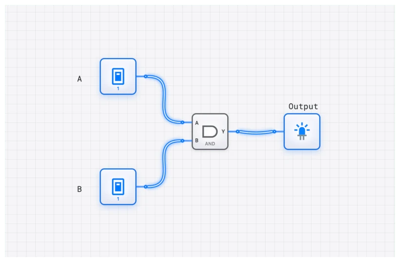
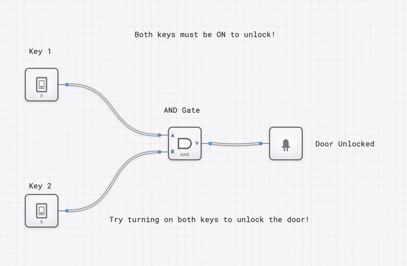
- AND: The gate of “All or Nothing.” An -input AND gate outputs a 1 if and only if every single input is 1.
- OR: The gate of “Any.” An -input OR gate outputs a 1 if at least one of its inputs is 1.
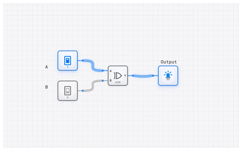
- XOR: The “Odd-Parity” gate. An -input XOR gate outputs a 1 if an odd number of its inputs are 1. This is a subtle but vital distinction from the 2-input version.
Technical Specification: The 3-Input AND Reference
To understand the scaling, let’s look at the truth table for a 3-input AND gate. For any -input gate, the truth table will have possible input combinations. As grows, the table expands exponentially, but the logic remains consistent.
| Input A | Input B | Input C | Output Y |
|---|---|---|---|
| 0 | 0 | 0 | 0 |
| 0 | 0 | 1 | 0 |
| 0 | 1 | 0 | 0 |
| 0 | 1 | 1 | 0 |
| 1 | 0 | 0 | 0 |
| 1 | 0 | 1 | 0 |
| 1 | 1 | 0 | 0 |
| 1 | 1 | 1 | 1 |
In this table, you’ll notice that only the final row—where all inputs are HIGH—results in a HIGH output. This “strictness” is what makes the AND gate the primary tool for address decoding and enable-signal generation.
Boolean Expressions and Scaling
The mathematical representation of these gates follows the standard laws of Boolean algebra, specifically the Associative Law. This law tells us that , which is the theoretical justification for building larger gates out of smaller ones.
For an -input AND gate:
For an -input OR gate:
For an -input XOR gate (Parity):
When we move into the realm of NAND and NOR, we apply De Morgan’s theorems to understand how they behave as they scale. An -input NAND is not just a series of NANDs; it’s an AND operation followed by a single NOT.
The Critical Trade-Off: Propagation Delay
In physical silicon, a “128-input AND gate” does not exist as a monolithic component. Standard logic families (74-series, CMOS cell libraries) provide 2-input, 3-input, and occasionally 4-input or 8-input gates. Anything wider must be built from smaller gates.
How you arrange those smaller gates determines the propagation delay () — the time for a change at the input to reach the output. If a single 2-input gate has a delay of , the total delay of your multi-input construction depends entirely on its structure.
Implementation Strategy A: The Cascade (The Slow Way)
The most intuitive way to build an 8-input AND gate is to chain them. You take the output of the first 2-input AND, feed it into the next, and so on.
In this “Cascade” structure, the signal from Input A must travel through seven consecutive gates to reach the output. The total delay is linear:
If is 1ns, your 8-input gate takes 7ns. That might not sound like much, but in a synchronous system, this delay limits your maximum clock frequency.
Implementation Strategy B: The Tree Structure (The Fast Way)
A “tree” or “tournament” structure pairs the inputs: A and B go to one gate, C and D to another, E and F to a third, and G and H to a fourth. The outputs of those four gates then feed into two gates in the next layer, which finally feed into one last gate.
The total delay now grows logarithmically:
For our 8-input gate: . The delay is only — less than half the cascade delay of 7ns.
Side-by-Side Comparison
| Metric | Cascade (n=8) | Tree (n=8) |
|---|---|---|
| Delay formula | ||
| Total delay | ||
| Gate count | ||
| Wiring complexity | Simple chain | Balanced binary tree |
Both structures use exactly the same number of gates ( for inputs). The tree is faster purely because it reduces the longest signal path from linear to logarithmic. The trade-off is slightly more complex routing, which matters in physical layout but is negligible in most designs.
Interactive Demo: Visualizing the Delay on digisim.io
The best way to understand the delay difference is to build both structures and observe them side by side.
- Setup: Place eight INPUT_SWITCH components on your canvas.
- The Cascade: Build a chain of seven AND gates. Connect the final output to an OUTPUT_LIGHT.
- The Tree: Below that, build the tree structure using seven AND gates. Connect its final output to a second OUTPUT_LIGHT.
- The Test: Turn all switches ON. Both lights turn on. Now, toggle the very first switch (Input A) OFF.
When using the OSCILLOSCOPE_8CH, you will see the “Tree” output transition noticeably faster than the “Cascade” output. This is the physical manifestation of the delay formula difference.
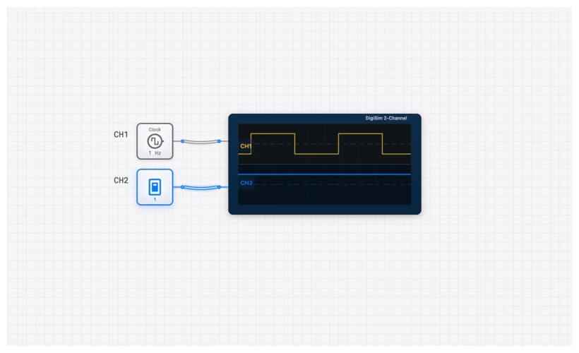
Oscilloscope Verification
Connect Channel 1 to the toggled input, Channel 2 to the tree output, and Channel 3 to the cascade output. The time offset between Channel 1 and Channel 2 represents , while the offset between Channel 1 and Channel 3 represents . This measurement technique — comparing signal arrival times on an oscilloscope — is the standard method for timing analysis in both simulation and real hardware debugging.
Real-World Applications
1. Memory Address Decoding (The Intel 8086 Example)
In classic architectures like the Intel 8086, the CPU needs to talk to specific chips. Imagine you have a RAM chip that should only respond when the address bus hits 0xFFFF0.
To detect this, you need a 20-input AND gate. Some inputs are inverted (using NOT gates) to match the zeros in the address, while others are direct. If you used a cascaded structure here, the “Chip Select” signal would arrive so late that the CPU might have already moved on to the next instruction. Architects always use tree-based decoders to ensure the memory responds within the required “access time.”
2. Data Bus Parity Generation
Reliability is everything. When sending a byte of data, we often add a “Parity Bit” to detect errors. An even parity bit is 1 if the number of 1s in the data is odd, making the total count even.
This is exactly what a multi-input XOR gate does.
By using a tree of XOR gates, you can generate a parity bit for a 64-bit data bus in just 6 gate delays (). This happens on every single memory write in high-end servers — see also our coverage of XOR vs XNOR in error detection.
Related Topics in the Curriculum
As you continue exploring digital logic on digisim.io, these related topics will deepen your understanding:
- Basic Logic Gates (The primitives)
- Boolean Algebra & De Morgan (The math)
- Propagation Delay & Timing Diagrams (The performance)
- Decoders (The primary application of multi-input AND)
Summary: Design Guidelines
| Guideline | Detail |
|---|---|
| Default to tree structures | Use balanced binary trees whenever propagation delay matters. The speed improvement is free — no extra gates required. |
| Respect fan-in limits | Physical gates degrade above 3-4 inputs due to increased capacitance. Use the tree structure’s natural 2-input fan-in. |
| Consider fan-out | Each gate output driving many inputs introduces additional delay. Buffer high-fan-out nodes. |
| Cascade when area is critical | In extremely area-constrained designs (e.g., dense FPGA routing), the simpler wiring of a cascade may be preferred if the delay is acceptable. |
| Simulate before committing | Use digisim.io with the OSCILLOSCOPE to measure actual propagation delay before finalizing your architecture. |
The jump from 2-input gates to multi-input systems is the first step into computer architecture — where correctness is necessary but performance is the real design challenge.
Continue with propagation delay and timing, or open the AND gate component reference and try wiring an 8-input tree against a cascade.